
Phone: +86-137 5102 2384
Phone: +86-137 5102 2384
High-Reliability PCB Assembly for Next-Generation Communication Electronics
In today’s connected world, communication devices such as Wi-Fi routers, 5G modules, IoT gateways, and telecom infrastructure equipment require extremely stable RF performance, precise impedance control, and high-density PCB assembly processes.
We provide one-stop PCB assembly services for OEMs and product developers, covering PCB fabrication, component sourcing, SMT & THT assembly, RF module integration, functional testing, programming, and box build assembly for communication electronics manufacturing projects.
|
Challenge
|
Our OEM Strategy
|
|
RF Performance
|
Utilization of Nitrogen Reflow Soldering to optimize solder joint wetting and
conductivity, minimizing RF signal attenuation.
|
|
Soldering Reliability
|
100% inspection using AOI and X-Ray for BGA and QFN packages to
eliminate cold joints, bridging, or hidden voids.
|
|
Supply Resilience
|
Global component sourcing network with real-time BOM risk alerts and verified
"Drop-in Replacement" suggestions to maintain production continuity.
|
Project Background: A client required OEM manufacturing for a Wi-Fi 6 router featuring a 4-layer high-density PCB with integrated 2.4G/5G dual-band modules and strict thermal requirements.
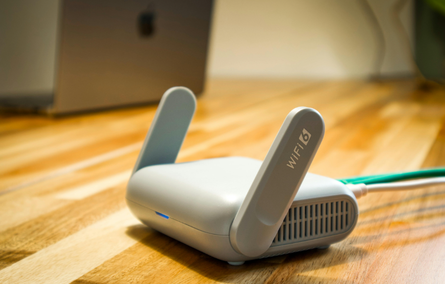
Communication devices rely on high-speed RF signals. Even minor impedance deviation or soldering inconsistency can result in signal loss, packet errors, or reduced transmission performance.
High-density PCBs with BGA and RF modules generate concentrated heat, requiring advanced thermal via design and precise heat dissipation control.
Communication PCBs often contain hundreds of components. Shortage of RF chips or MCUs can disrupt production schedules without strong supply chain management.
Modern communication devices require ultra-compact layouts using 0201 components and HDI structures with extremely tight assembly tolerances.
We support controlled impedance PCB assembly with ±5% tolerance for high-speed differential signal integrity in communication systems.
Nitrogen reflow technology improves solder wetting quality and reduces oxidation, ensuring stable RF performance and long-term reliability.
High-accuracy SMT placement for 0201 components, BGA, QFN, and RF shielding structures used in communication electronics.
We manage multi-layer, high-component-count BOMs for communication devices with stable procurement and production continuity.
Reliable sourcing for RF chips, MCUs, and long-lead components with verified global supply channels.
We provide drop-in replacement recommendations to avoid production delays caused by component shortages.
Looking for a reliable communication PCB assembly manufacturer for RF, telecom, or IoT devices?
We provide engineering support, DFM optimization, and scalable production from prototype to mass production.
Contact us today for a professional evaluation of your communication electronics project.

Find Partners, Not Just Suppliers
Expert OEM & PCBA manufacturing tailored to your exact specifications. Contact us today to discuss your project and discover a more collaborative way to manufacture.
Get a Fast Quote & Free DFM Review
Related PCB Assembly Service







