
Phone: +86-137 5102 2384
Phone: +86-137 5102 2384
Sep. 18, 2026
Share:
A hidden solder defect beneath a Ball Grid Array (BGA) package can disable an otherwise perfect PCB without leaving any visible evidence. During production, a BGA may contain hundreds or thousands of solder joints hidden between the package and the board. Conventional Automated Optical Inspection (AOI) cannot directly see these joints, while electrical testing may identify a failure without revealing its cause. This is why Why X-Ray Inspection Is Important for BGA PCB Assembly is not simply a process question—it is a reliability, warranty, and supply-chain risk question. At Benewave, we use X-ray inspection as part of a controlled one stop pcb assembly workflow to identify voiding, opens, shorts, insufficient solder, and misalignment before products reach the customer.
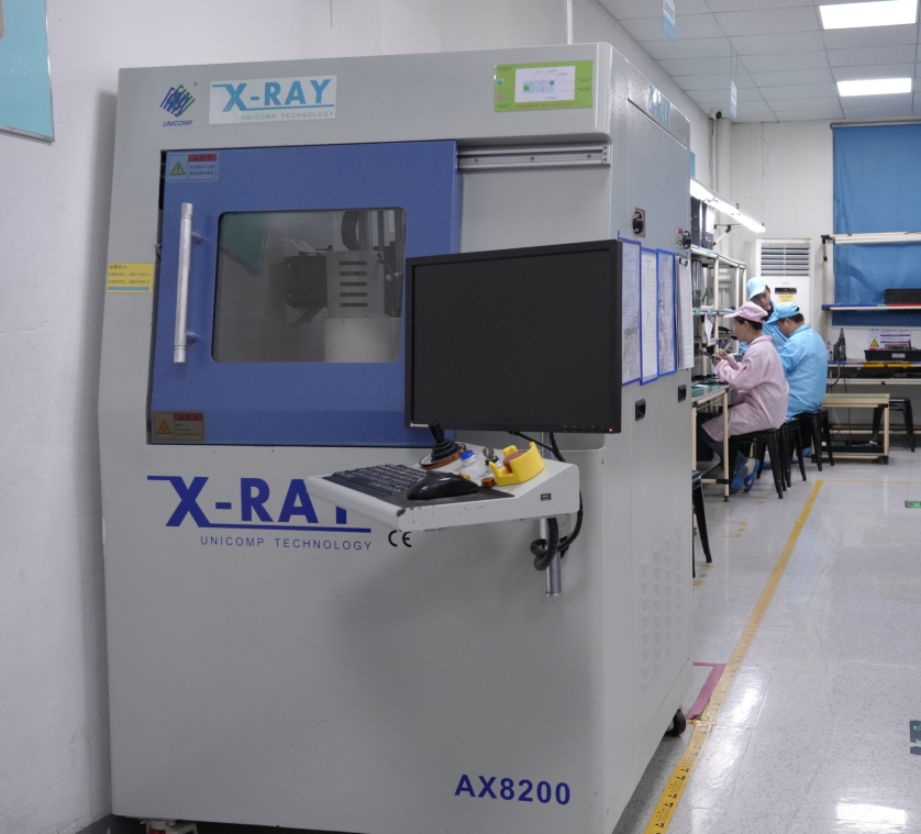
BGA technology improves electrical performance and saves board space, but it also creates a serious inspection challenge. The solder balls are arranged beneath the component body, so the most critical interconnections are physically concealed.
X-ray inspection uses differences in material density to create an image of the solder joints. Depending on the equipment and application, 2D X-ray or 3D Computed Tomography (CT) can reveal:
When customers ask us Why X-Ray Inspection Is Important for BGA PCB Assembly, the most practical answer is simple: it provides visibility where optical inspection cannot.
AOI is valuable for checking component placement, polarity, visible solder fillets, and surface defects. However, it cannot reliably inspect the solder joints under a BGA package.
In-Circuit Test (ICT) and Functional Testing (FCT) are also important, but they generally indicate whether a circuit behaves correctly at a specific moment. They may not expose a latent defect that fails after:
X-ray inspection complements AOI, ICT, and FCT rather than replacing them. A robust process uses each method for the defect types it is best equipped to detect.
Understanding the root causes helps manufacturers prevent defects instead of only sorting them after assembly.
BGA reliability begins with solder paste printing. Stencil aperture design, paste rheology, squeegee pressure, print speed, and board support all affect deposit volume.
Common problems include:
A small variation in solder paste volume can become a significant defect after reflow.
The reflow profile must match the solder alloy, component package, PCB layer structure, and thermal mass. Excessive ramp rate may cause solder splatter or component stress. Insufficient soak time can contribute to poor activation, while an incorrect peak temperature may produce incomplete reflow.
For lead-free SAC alloys, process engineers typically control parameters such as:
The correct limits should be defined according to the solder-paste supplier’s technical data and the customer’s assembly specification.
Package warpage can cause some solder balls to contact the PCB while others remain partially open. This is a known contributor to Head-in-Pillow (HiP) defects, particularly in large packages and lead-free processes.
PCB thickness, copper distribution, moisture absorption, component storage, and reflow temperature all influence warpage.
Voids are gas-filled spaces inside a solder joint. They may originate from solder paste volatiles, flux chemistry, pad design, or reflow conditions.
A void does not automatically mean a product must be rejected. Acceptance depends on:
For power BGAs, large voids can increase thermal resistance and reduce heat dissipation. For high-reliability applications, even moderate voiding may require engineering review.
Moisture-sensitive devices, damaged solder balls, incorrect placement force, and feeder variation can all affect joint formation. Components should be stored and handled according to applicable moisture sensitivity requirements, including the relevant JEDEC standards such as J-STD-033.
Benewave provides a coordinated manufacturing process rather than treating X-ray as an isolated final check. Our one stop pcb assembly model can include engineering review, component sourcing, SMT placement, BGA reflow, X-ray inspection, AOI, testing, and delivery coordination.
Design and manufacturability review
We examine BGA pitch, pad geometry, thermal relief, stencil requirements, component spacing, and access for test.
Solder paste and stencil control
Stencil thickness, aperture reduction, nano-coating, and paste selection are evaluated according to the component and assembly design.
Controlled SMT placement
Placement accuracy, feeder performance, component orientation, and package handling are monitored.
Profile verification
Thermocouples and profile records are used to confirm that the reflow process is suitable for the board’s thermal mass.
X-ray examination
BGA joints are inspected for voiding, opens, bridges, misalignment, and other hidden anomalies. When required, 3D X-ray provides sectional and volumetric analysis.
Defect classification and root-cause analysis
Findings are compared with IPC requirements, customer specifications, and engineering criteria. Corrective action may include printer adjustment, stencil modification, profile optimization, or component review.
Traceable reporting
Inspection images, lot information, operator records, and corrective-action data are maintained for quality review.
For critical assemblies, Benewave can support 100% X-ray inspection of designated BGA components rather than relying only on sampling. Equipment configured for high-resolution work may identify features with measurement resolution down to 0.01 mm, although actual accuracy depends on magnification, board thickness, geometry, calibration, and the inspection system.
We also aim to provide a 24-hour response for engineering questions and inspection feedback, subject to project complexity and information availability. Fast communication matters because an unresolved BGA defect can stop downstream production.
A credible inspection program should be tied to recognized standards instead of informal visual judgment.
Relevant references may include:
These standards do not mean every BGA must meet one universal void percentage or inspection rule. Acceptance criteria should be agreed before production, especially for automotive, aerospace, medical, telecom, and high-power electronics.
Consider a production lot of 1,000 BGA boards. If a hidden defect rate is only 2%, approximately 20 boards may contain a solder-joint problem. Without X-ray inspection, those boards may pass visual inspection and enter system-level testing or customer shipment.
The financial impact can include:
| Business stage | Potential impact |
|---|---|
| Assembly line | Rework, line stoppage, and additional labor |
| System integration | Troubleshooting time and delayed delivery |
| Customer site | Field failure, service visits, and replacement units |
| Brand reputation | Reduced confidence and lost future orders |
| Regulated product | Documentation gaps, corrective-action investigations, or recalls |
This is an illustrative calculation, not a claim about a specific Benewave customer. Its purpose is to show why a small hidden defect rate can create a disproportionate commercial cost.
In many cases, the cost of detecting a defect during PCB assembly is far lower than finding it after enclosure integration or field deployment. For this reason, Why X-Ray Inspection Is Important for BGA PCB Assembly should be evaluated through total cost of quality, not only inspection price.
Ignoring hidden BGA inspection can create several layers of risk.
A marginal solder joint may initially conduct electricity but fail after thermal expansion and contraction. Differences in the Coefficient of Thermal Expansion (CTE) between the silicon package, substrate, solder, and PCB can create fatigue over time.
Potential outcomes include:
When product demand changes, customers often move quickly from prototype quantities to mass production. A process that appears acceptable at low volume may become unstable at higher throughput if inspection and traceability are not scalable.
Neglecting X-ray can also weaken:
We recommend that customers define the inspection strategy before releasing the PCB to production.
A practical plan may combine:
Why X-Ray Inspection Is Important for BGA PCB Assembly becomes clear when we consider what is hidden beneath the package: critical solder joints that cannot be confirmed through ordinary visual inspection. Defects caused by paste printing, reflow instability, warpage, voiding, or placement variation can become expensive field failures if they are not detected early.
At Benewave, we combine X-ray inspection with engineering review, SMT process control, AOI, electrical testing, documented standards, and responsive communication. Whether you need prototype support or a scalable one stop pcb assembly partner, ask for a defined BGA inspection plan, measurable acceptance criteria, and traceable quality records.
If your product includes BGA, QFN, power modules, or other hidden solder connections, contact Benewave before production begins. Early inspection planning can protect yield, reliability, delivery schedules, and customer trust.
Find Partners, Not Just Suppliers
Expert OEM & PCBA manufacturing tailored to your exact specifications. Contact us today to discuss your project and discover a more collaborative way to manufacture.
Get a Fast Quote & Free DFM Review
Related PCB Assembly Service







