In the world of electronics manufacturing, there is a massive difference between a circuit board that works on a computer screen and one that can be successfully mass-produced on a factory floor. A design can pass every electrical simulation in your EDA software, yet completely stall the moment it hits an automated assembly line.
For hardware startups and established engineering teams alike, the bridge between an ideal design and a flawless physical product is DFA (Design for Assembly) checking.
What Exactly is DFA Checking in PCBA?
Design for Assembly (DFA) is a specialized engineering methodology and review process focused entirely on how easily, quickly, and reliably electronic components can be integrated and soldered onto a bare printed circuit board. While traditional electrical simulations and testing verify whether a circuit functions conceptually from a logical standpoint, a DFA check evaluates whether the physical layout of the board is optimized for automated manufacturing machinery and high-yield factory throughput.
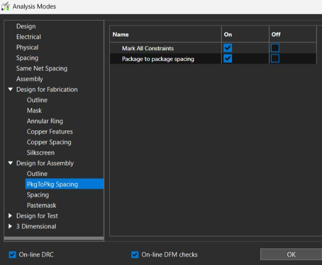
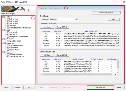
When design files (such as Gerber files, ODB++ databases, or IPC-2581 formats) are submitted to a manufacturing partner, assembly engineers use advanced, specialized DFA software to simulate the entire physical assembly process before a single piece of hardware is touched. This digital audit analyzes the board in three dimensions. It inspects the precise positioning of every resistor, capacitor, integrated circuit (IC), ball grid array (BGA), transistor, and connector, comparing the layout against hundreds of known, real-world manufacturing constraints and machine limitations.
In modern electronics manufacturing, human hands rarely solder components onto mass-produced circuit boards. Instead, highly synchronized, automated assembly lines do the heavy lifting. The process follows a strict sequence:
Solder Paste Printing → Automated Component Placement → Reflow Soldering → Inspection and Testing.
A thorough DFA check ensures that these automated systems can execute their jobs flawlessly. It guarantees that robotic nozzles have the clearance to drop off parts without colliding, stencils can release solder paste accurately without clogging, reflow ovens heat components uniformly, and inspection cameras have a clear line of sight to verify every solder joint. In short, DFA transforms a schematic into a manufacturable reality.
What are the Differences Between PCB DFM and PCBA DFA?
In the electronics industry, terms like DFM (Design for Manufacturing), DFF (Design for Fabrication), and DFA (Design for Assembly) are frequently thrown around, conflated, or used interchangeably. This causes significant confusion for product designers and procurement teams alike. However, PCB DFM and PCBA DFA address two completely distinct, sequential stages of the hardware production ecosystem. To optimize a product for yield and cost, it is vital to understand where one process ends and the other begins.
1. PCB DFM (Design for Fabrication)
PCB DFM—frequently referred to as DFF—is strictly focused on the creation of the bare, unpopulated circuit board. At this stage of the process, electronic components do not exist. Instead, the review deals purely with raw materials: fiberglass substrates (like FR4), copper foils, resin prepregs, chemical plating solutions, protective solder masks, and silkscreen inks.
A DFM check evaluates whether the fabrication plant can physically print the circuit layers, laminate them together under high pressure and temperature, chemically etch the copper traces, and drill the necessary vias without causing structural failures. A DFM engineer looks for tight spacing that could cause copper shorts, thin traces that could break or over-etch, and improper drill-to-copper ratios that could slice through internal circuits. If the bare board cannot be built reliably, the project stops here.
2. PCBA DFA (Design for Assembly)
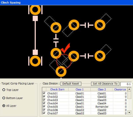
Conversely, PCBA DFA assumes that the bare board can be—and has been—fabricated flawlessly. Its sole focus is the populated board—the process of taking that raw copper-and-fiberglass base and successfully assembling the Bill of Materials (BOM) onto it.
DFA looks at the interplay between the board's surface features and the physical components themselves. It analyzes component spacing, pad geometries, land pattern footprints, component heights, thermal dynamics, and orientation on the panel. While PCB DFM ensures you have a physical board to work with, PCBA DFA ensures that your components can actually be securely, rapidly, and permanently attached to that board by mass-production machinery.
| Feature Comparison |
PCB DFM (Fabrication) |
PCBA DFA (Assembly) |
| Primary Focus |
The raw, unpopulated copper board |
The final, fully populated board with components attached |
| Core Materials Evaluated |
Fiberglass (FR4), copper foil, solder mask, laminates |
Bare PCBs, electronic components (chips, passives), solder paste |
| Typical Issues Identified |
Narrow traces, acid traps, improper drill aspect ratios, copper slivers |
Component collisions, tombstoning, solder bridging, component orientation errors |
| Key Factory Equipment |
Laser drills, chemical etching tanks, lamination presses, plating baths |
Solder paste stencils, pick-and-place robots, reflow ovens, AOI machines |
| Primary Yield Impact |
Bare board survival rate and electrical continuity of raw layers |
First-Pass Yield (FPY) of the complete, working electronic assembly
|
Why DFA checking is essential for PCBA?
1. Drastically Reduces Manufacturing Defects
Automated high-speed soldering is a highly sensitive process governed by the laws of thermodynamics, fluid dynamics, and surface tension. When components are packed tightly onto a dense modern circuit board, minor layout oversights that look benign in a CAD tool turn into systemic defects on the production line. A rigod to catch and eliminate these issues beforehand.
Tombstoning
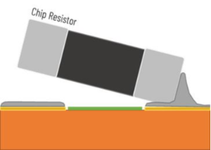
This common defect occurs primarily with small surface-mount passives, such as 0402 or 0201-sized resistors and capacitors. If the copper pads for a component are unevenly sized, or if one pad connects directly to a wide trace while the other connects to a thin trace, heat will distribute unevenly during the reflow process. The solder paste on one pad melts fractions of a second faster than the other. The wetting force and surface tension of the molten solder pull harder on that single side, causing the component to literally lift off the opposite pad and stand upright like a tombstone. DFA checks identify pad imbalances to prevent this.
Solder Bridging
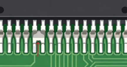
When the leads or pins of fine-pitch components (like microcontrollers or QFP packages) are placed too close together, or if the land pattern doesn't include a sufficient solder mask dam between the pads, molten solder can cross the gap. This creates a "bridge" or short circuit between pins. Solder bridging can render a board entirely non-functional or, worse, cause electrical shorts that damage expensive silicon chips during power-up. DFA software instantly flags areas where component pitch puts the design at risk for bridging.
2. Lowers Production and Rework Costs
In manufacturing, there is a golden rule: the cost of fixing a defect increases tenfold at each subsequent stage of production. Catching a layout error during the digital design phase costs almost nothing. Catching it after the board is assembled costs a fortune.
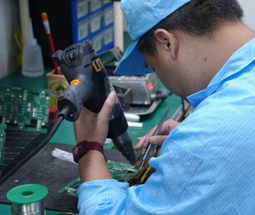
If a design defect passes through assembly unchecked and causes a 25% failure rate during inspection, the financial impact is severe. Every failing board must be pulled off the automated line and sent to a manual rework station. Here, a highly skilled technician must use a hot-air rework station or soldering iron to manually desolder the faulty components, clean the coppe r pads, reapply solder, and manually place a new component.
This process is incredibly labor-intensive, drastically slowing down production throughput. Furthermore, subjecting a localized area of a PCB to repeated manual heating introduces the risk of thermal stress, which can warp the board, lift copper pads, or damage sensitive internal IC structures. By ensuring a high First-Pass Yield (FPY), DFA checking ensures that the vast majority of your boards cross the automated line perfectly the first time, protecting your budget from expensive labor and scrap costs.
3. Prevents Mechanical Collisions and Space Constraints
EDA software typically displays PCB layouts in 2D top view. Though 3D modes are available, vertical space issues are often ignored amid dense circuitry.
Electronic components operate in a 3D environment, so volumetric clearance check is a core part of DFA. Tall parts like electrolytic capacitors and vertical connectors may collide with nearby SMD components during high-speed pick-and-place, leading to damage and placement errors.
In addition, tall components cause thermal shadowing in reflow soldering, resulting in insufficient heating for adjacent parts. They also block AOI cameras, making solder joint inspection impossible in shadowed areas.
4. Optimizes Thermal Management During Soldering
Uniform reflow temperature across all solder joints is essential for reliable connections. Yet PCB materials and components vary greatly in heat absorption, making thermal optimization a key part of DFA.
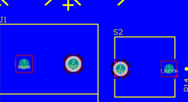
Pads connected to large copper ground planes act as strong heat sinks. They draw heat away quickly in the reflow oven, leading to cold solder joints. Such joints appear normal but are fragile, with poor conductivity and high failure risks under vibration or temperature changes.
DFA detects these risks and requires thermal relief pads. Thin copper spokes limit heat loss during soldering, ensuring full solder melting while keeping stable electrical connectivity.
5. Accelerates Your Time-to-Market
In the competitive hardware industry, fast time-to-market is critical. Even short delays can lead to lost market opportunities.
DFA flaws in PCB designs will prompt manufacturers to pause production and send Engineering Queries (EQs), causing lengthy back-and-forth communications and schedule delays. In severe cases, unaddressed design issues result in incompatible footprints, leading to full board scrappage and repeated fabrication.
Thorough DFA checks before production eliminate such risks, streamlining the entire manufacturing process.
Conclusion
In modern electronics manufacturing, the metrics that dictate a successful product lifecycle are speed, premium build quality, and cost-efficiency. Achieving a functional, high-performance circuit schematic is a monumental engineering milestone, but a product cannot achieve commercial viability if it cannot be manufactured reliably and cost-effectively at scale.
By prioritizing PCBA DFA checking at the inception of your production planning, you protect your hardware project from catastrophic design re-spins, eliminate entirely preventable assembly defects, and minimize expensive manual rework. Partnering with an experienced electronics manufacturing services (EMS) provider that places a heavy, uncompromising emphasis on pre-production DFA reviews is the ultimate insurance policy for your hardware. It is the single best way to guarantee your product hits the market exactly on time, strictly on budget, and built to the highest standards of long-term reliability.
As a professional PCBA manufacturer, Benewave conducts thorough DFA checks for all projects prior to component sourcing and fabrication. Feel free to contact us if you have any requirements.
Resources
Here are a list of some PCB CAD programs, some of them could be used for DFM and DFA checking, compiled by ElCap from EEVblog Forum:
https://www.eevblog.com/wiki/index.php?title=PCB_CAD_programs