Phone: +86-137 5102 2384
Phone: +86-137 5102 2384
Oct. 19, 2026
Share:
Automated Optical Inspection (AOI) is essential for identifying visible assembly defects, but it is not sufficient when a PCB contains hidden solder joints, internal structural defects, electrical faults, or functional problems that only appear under operating conditions. For reliable production, buyers should combine AOI with suitable methods such as X-ray inspection, in-circuit testing, and functional testing according to the board design and risk level. As part of Benewave’s one-stop PCB assembly service, inspection and testing can be coordinated with PCB fabrication, component sourcing, SMT/DIP assembly, programming, and final integration.
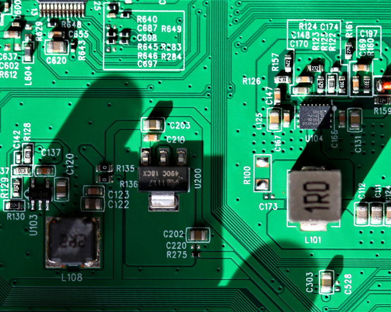
AOI uses cameras and image-processing software to inspect visible features on an assembled circuit board. Depending on the equipment and inspection program, it can identify issues such as missing components, incorrect polarity, component misalignment, lifted leads, and visible soldering defects.
However, AOI cannot verify every aspect of PCB quality. The key limitation is that optical inspection evaluates what the camera can see, rather than every internal connection or the complete electrical behavior of the product.
Ball Grid Array (BGA) packages use solder balls beneath the component body. Similar inspection challenges can occur with other bottom-terminated packages, including some Land Grid Array (LGA) and Quad Flat No-Lead (QFN) components.
Because these connections are concealed after assembly, a standard optical camera cannot directly inspect their solder joints. A component may look correctly positioned from above while its hidden connections contain bridging, insufficient solder, or other defects.
Recommended method: X-ray inspection, also known as Automated X-ray Inspection (AXI), can reveal many hidden solder-joint problems that surface-level AOI cannot identify. The inspection criteria should reflect the package type, board design, and applicable acceptance requirements.
A solder joint may appear acceptable externally but contain internal voids or other defects. These issues can affect electrical continuity, mechanical strength, or thermal performance, depending on the component and application.
Three-dimensional AOI can provide more information about visible solder geometry than conventional two-dimensional inspection, but it still does not directly reveal every internal defect. X-ray inspection can help assess hidden solder structures, although its ability to detect particular cracks or defects depends on the defect geometry, material contrast, equipment, and inspection setup.
Recommended method: Use X-ray inspection for suitable hidden-joint applications and apply additional electrical or reliability tests when the product’s risk assessment requires them.
A resistor, capacitor, or integrated circuit may be mounted in the correct position and orientation but still be electrically incorrect or defective. For example, a passive component could have the wrong value, or a circuit could contain an open connection or short circuit that is not visually apparent.
AOI can check markings and component placement when these features are visible and supported by the inspection program. It cannot reliably establish every component’s actual electrical value or confirm that all circuit nodes behave as designed.
Recommended methods:
In-Circuit Testing (ICT) can check accessible circuit nodes, shorts, opens, and certain component values, depending on the test fixture and circuit design.
Flying-probe testing can provide electrical checks without a dedicated bed-of-nails fixture, making it useful for many prototype and lower-volume applications.
Functional Circuit Testing (FCT) can verify whether the assembled product performs specified operations under defined test conditions.
The right method depends on test-point access, circuit complexity, production volume, and required fault coverage.
Multilayer boards contain internal copper layers, buried vias, and connections that cannot be examined directly using surface-level optical inspection. Potential problems include internal connection defects, shorts between layers, and delamination.
AOI may identify visible surface issues, but it cannot independently verify every buried connection or internal laminate structure.
Recommended method: Depending on the suspected defect, manufacturers may use electrical continuity or isolation testing, flying-probe testing, X-ray inspection, or specialized failure-analysis techniques. No single method identifies every type of internal PCB defect, so the test plan should be matched to the construction and failure risk.
A board can pass visual inspection and basic electrical checks yet fail when powered on. Firmware may not load correctly, communication interfaces may malfunction, sensors may return incorrect readings, or the assembled device may fail to meet its operating requirements.
AOI does not verify these behaviors because it does not run the product through its intended operating sequence.
Recommended method: Functional testing can verify defined operating conditions, interfaces, outputs, and other product-specific requirements. Where relevant, firmware programming, communication checks, and application-specific tests should be included in the production plan.
For products with wireless connectivity, additional RF tests may be needed. The exact test coverage depends on the product specification rather than AOI capability alone.
| Inspection or test method | Main purpose | Important limitation |
|---|---|---|
| AOI | Visible component placement, polarity, and soldering defects | Cannot directly inspect concealed joints or prove full electrical functionality |
| 3D AOI | More detailed measurement of visible component and solder geometry | Does not reveal every internal solder defect |
| X-ray / AXI | Inspection of hidden solder joints and certain internal structures | Detectability depends on geometry, materials, and inspection setup |
| ICT | Electrical checks, including accessible nodes and selected component values | Requires suitable test access and coverage |
| Flying-probe testing | Electrical verification without a dedicated bed-of-nails fixture | Test time and coverage depend on board design and production needs |
| Functional testing (FCT) | Verification of defined powered operating behavior | Tests only the functions and conditions included in the test plan |
For many electronic products, these methods complement rather than replace one another. AOI is useful for rapid visual checks, X-ray addresses hidden features, electrical tests evaluate circuit integrity, and FCT verifies selected operating functions.
The most effective inspection plan starts with the product’s risks and acceptance requirements instead of adding every possible test to every board.
Identify BGA, QFN, LGA, fine-pitch components, dense layouts, and other features that create inspection challenges. Review test-point accessibility and determine whether the board requires special fixtures or additional verification.
During supplier selection, ask whether the manufacturer can review the design for manufacturability and coordinate fabrication, assembly, and testing. Benewave provides integrated services through its one-stop PCB assembly solution, helping buyers coordinate these manufacturing stages with one supplier.
Specify which defects must be checked, which components require X-ray inspection, and what electrical or functional tests are necessary. Clarify whether inspections apply to every board, selected samples, or particular production stages.
Avoid assuming that a statement such as “AOI inspected” means the product has passed hidden-joint inspection, electrical testing, and functional verification. Request a clear description of the actual test coverage.
Inspection is most useful when failures lead to documented investigation and process correction. If AOI repeatedly identifies shifted components, the assembly process may need adjustment. If X-ray reveals recurring soldering defects, the team may need to review stencil design, paste deposition, component placement, or the reflow profile.
When electrical or functional tests fail, the investigation should consider component quality, solder connections, circuit design, firmware, and test-fixture reliability as appropriate.
Before placing a production order, agree on the required inspection records and acceptance criteria. Depending on the project, documentation may include inspection results, electrical test reports, functional test records, defect classifications, and corrective-action reports.
The buyer and manufacturer should also define how nonconforming boards are handled, how retesting is controlled, and what evidence is required before shipment.
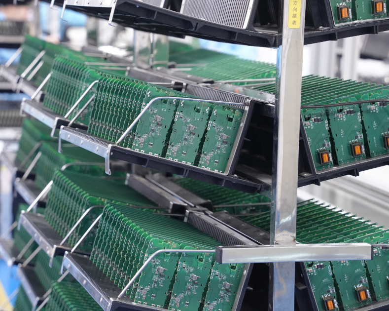
Benewave provides turnkey PCBA services covering PCB fabrication, electronic component sourcing, SMT and DIP assembly, programming, functional testing, and box build integration. Its manufacturing capabilities include six SMT lines, three DIP lines, and dedicated functional-testing lines, supporting projects from rapid prototyping through mass production.
For assemblies that require more than visible inspection, Benewave’s quality workflow can incorporate AOI, X-ray inspection, in-circuit testing, and functional testing according to project requirements. The purpose is to match each inspection method to the defects it can realistically detect rather than treating one inspection technology as a substitute for all other checks.
Benewave supports electronics applications including consumer electronics, smart-home and IoT products, industrial electronics, medical devices, automotive electronics, and communication equipment. Since inspection requirements vary significantly between these applications, buyers should communicate their component list, PCB files, expected production volume, operating environment, and required acceptance criteria before manufacturing begins.
No. AOI examines visible features, while X-ray can reveal many hidden solder-joint structures. Boards with concealed connections may need both methods, depending on the design and quality requirements.
No. AOI can detect many visible soldering and placement defects, but it cannot directly inspect every internal feature. Some hidden defects require X-ray or other verification methods.
Not always. ICT is useful when the circuit provides suitable access and the required tests can be implemented. Flying-probe or functional testing may be more appropriate for certain designs or production volumes.
No. FCT verifies the functions and operating conditions included in the test plan. It does not guarantee freedom from every latent defect or failure that could occur under untested conditions.
Prepare Gerber files, a bill of materials (BOM), assembly drawings, quantities, component package details, and any required inspection, electrical-testing, firmware, or functional-test specifications. Providing this information early helps the manufacturer assess process requirements and identify potential inspection gaps.
For your next PCB assembly project, contact Benewave at zoe@benewavetech.com to discuss your board design, hidden-joint inspection needs, electrical verification, and functional-testing requirements. Benewave can help you plan an appropriate quality-control workflow from PCB fabrication and component sourcing through assembly and final testing.
Find Partners, Not Just Suppliers
Expert OEM & PCBA manufacturing tailored to your exact specifications. Contact us today to discuss your project and discover a more collaborative way to manufacture.
Get a Fast Quote & Free DFM Review
Related PCB Assembly Service