Phone: +86-137 5102 2384
Phone: +86-137 5102 2384
Oct. 19, 2026
Share:
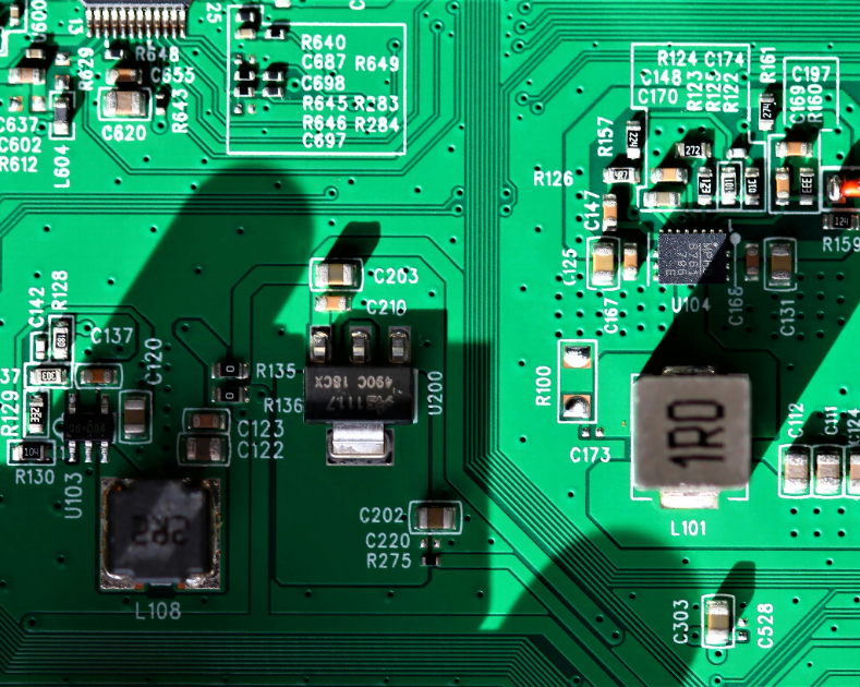
A modern SMT production line can handle components ranging from miniature 01005 chip passives to fine-pitch ICs, BGAs, QFNs, connectors, and other larger or irregularly shaped parts. However, the actual size range and placement reliability depend on the pick-and-place machine, feeder and nozzle configuration, vision system, PCB layout, and soldering process. For projects involving miniature components or dense layouts, buyers should review the manufacturer's capabilities before production. Benewave’s SMT and DIP assembly services support fine-pitch and high-density PCB assembly, including 01005 components, BGA and QFN packages, with inspection and testing options matched to project requirements.
Component size is not determined by the SMT line as a whole. It depends primarily on the capabilities of the placement machine and whether the production process can consistently print solder paste, pick up the component, align it, and solder it without creating defects.
Small passive components are common in compact consumer electronics, wearable devices, wireless modules, and IoT products.
Two package codes are particularly important:
0201 imperial: approximately 0.6 × 0.3 mm.
01005 imperial: approximately 0.4 × 0.2 mm.
These are imperial package designations. Their metric equivalents are commonly called 0603 and 0402, respectively, so buyers should always confirm the unit system used in the BOM and assembly drawings.
Placing such small components requires more than a machine that can physically pick them up. The feeder must present the parts consistently, the nozzle must match the package, and the vision system must locate the component accurately. Solder paste volume, pad geometry, component spacing, and reflow conditions also influence the final result.
Potential defects include tombstoning, component shifting, solder bridging, and insufficient or excessive solder.
Benewave supports miniature component assembly for compact electronics. Its consumer electronics PCB assembly solution addresses high-density layouts and small components used in products such as wearables, portable electronics, smart sensors, and charging devices.
SMT production lines can also assemble integrated circuits with closely spaced leads or solder connections beneath the package. Common examples include:
QFP: Quad Flat Package, with leads extending from the package sides.
QFN: Quad Flat No-Lead, with terminals around or beneath the package.
BGA: Ball Grid Array, with solder balls arranged beneath the package.
CSP and WLCSP: Chip-scale and wafer-level chip-scale packages used in space-constrained designs.
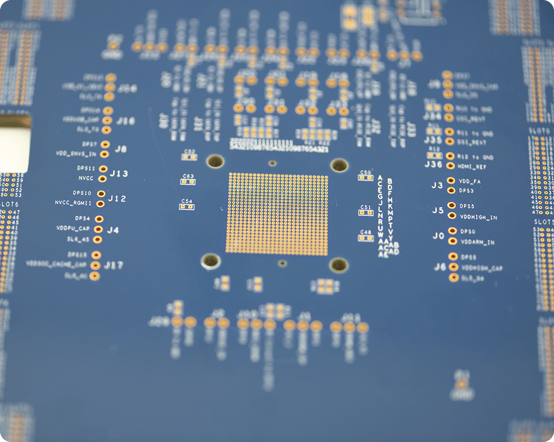
For these packages, the relevant specification is not just the overall component length and width. Lead pitch, ball pitch, pad design, solder-mask clearance, PCB warpage, and inspection access all affect manufacturability.
A BGA measuring 10 mm square with a 0.5 mm ball pitch presents different assembly challenges from a larger package with wider spacing. Similarly, a QFN with a central thermal pad may require careful stencil design and solder-volume control.
Benewave's one-stop PCB assembly service supports complex component assembly, including BGA and QFN packages. For fine-pitch projects, buyers should confirm the exact package, pitch, board layout, and inspection requirements during the engineering review.
Not every surface-mount component is miniature. Some boards use large connectors, power inductors, transformers, switches, shielding components, or other parts that require specialized handling.
Whether these parts can be placed automatically depends on several factors:
Component length, width, height, and weight.
Package shape and the availability of a suitable vacuum nozzle or mechanical gripper.
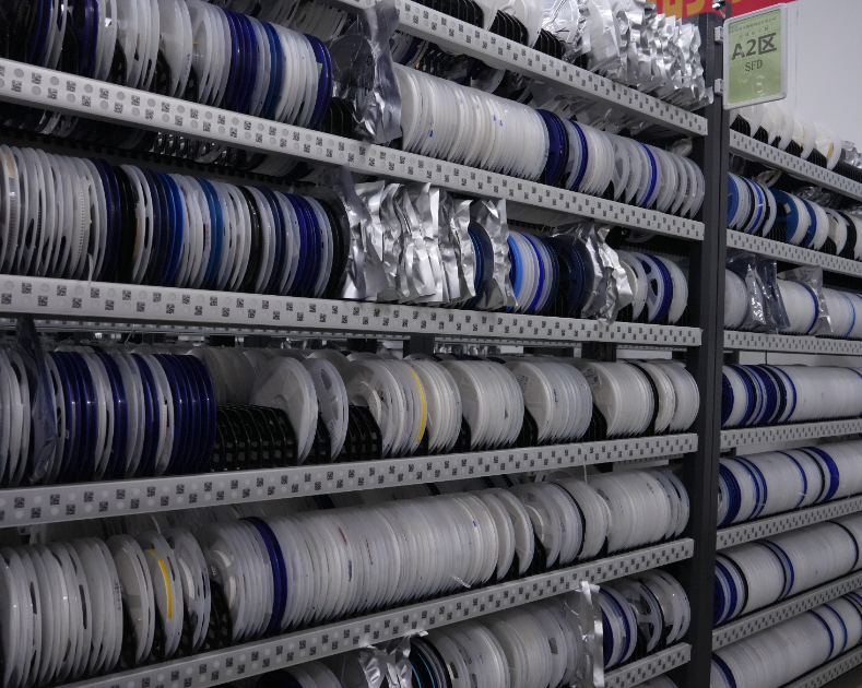
Tape-and-reel, tray, tube, or other feeder format.
Machine head clearance and placement-force limits.
Component orientation and surrounding PCB clearance.
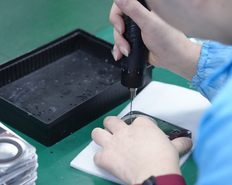
Some large components are suitable for automatic SMT placement, while others are better handled by specialized equipment, manual placement, or a through-hole process. A connector that appears compatible by size alone may still require a different mounting method because of its pins, mechanical load, or thermal requirements.
The distinction between SMT and through-hole assembly is especially important for large connectors and transformers. Benewave provides both SMT and DIP assembly, allowing the manufacturing process to be selected according to the component design rather than forcing every part into one mounting method.
The following table summarizes common component categories. It is a practical guide rather than a universal equipment specification.
| Component category | Typical examples | Main assembly consideration |
|---|---|---|
| Ultra-small passive | 01005, 0201 | Precise pickup, alignment, solder-paste control |
| Standard passive | 0402, 0603, 0805, 1206 | Feeder compatibility, polarity where applicable, spacing |
| Fine-pitch IC | QFP, QFN, CSP | Lead or terminal pitch, stencil design, alignment |
| Area-array IC | BGA, WLCSP | Ball pitch, PCB pad design, hidden-joint inspection |
| Large SMT component | Power inductors, some connectors, shields | Component height, weight, nozzle and clearance |
| Through-hole or mixed-technology component | Large connectors, terminal blocks, some transformers | DIP insertion, soldering process, mechanical requirements |
The actual limits must be checked against the selected equipment and the component datasheets. Package names alone do not establish that a part can be placed reliably.
Different machines are optimized for different production needs. High-speed placement equipment is effective for large quantities of common passive components, while flexible or high-precision machines may be better suited to fine-pitch ICs, unusual packages, and frequent product changes.
For a project using 01005 passives alongside BGAs and large connectors, the supplier should confirm that the line can accommodate all package types and explain how components outside the automatic placement range will be handled.
Ask for the machine's supported component dimensions, minimum package size, placement accuracy specification, and relevant process limitations. Avoid treating a headline placement-speed figure as proof that every component can be assembled at the same speed or accuracy.
Small components can be difficult to pick consistently if the feeder presents them incorrectly or the nozzle does not match their size and shape. Larger or irregular components may require special nozzles, tray feeders, or alternative handling methods.
Before production, the manufacturer should review the component package, part orientation, packaging format, and placement data. This helps identify components that may need special handling before the production run begins.
Machine vision helps locate components and correct placement coordinates. Its effectiveness depends on camera resolution, lighting, component surface characteristics, fiducial quality, and the machine's alignment method.
For miniature or fine-pitch parts, the PCB design must provide suitable alignment references. Poorly defined fiducials, incorrect component rotation data, or inconsistent footprints can cause placement problems even when the machine itself is capable.
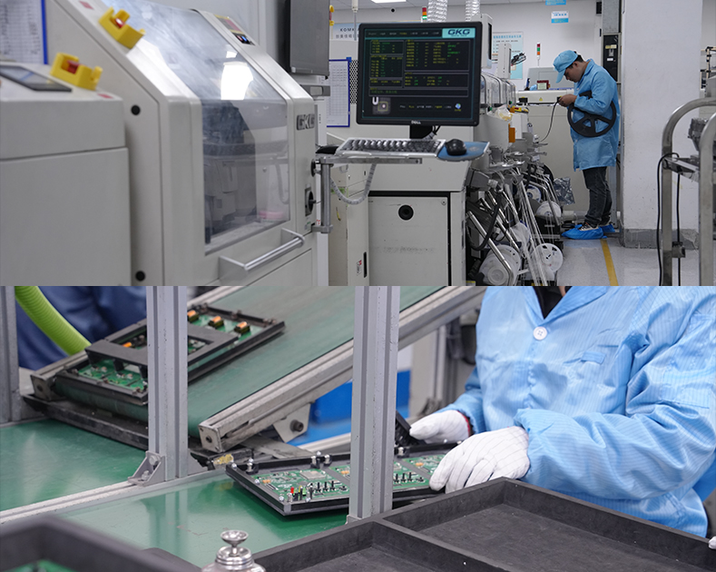
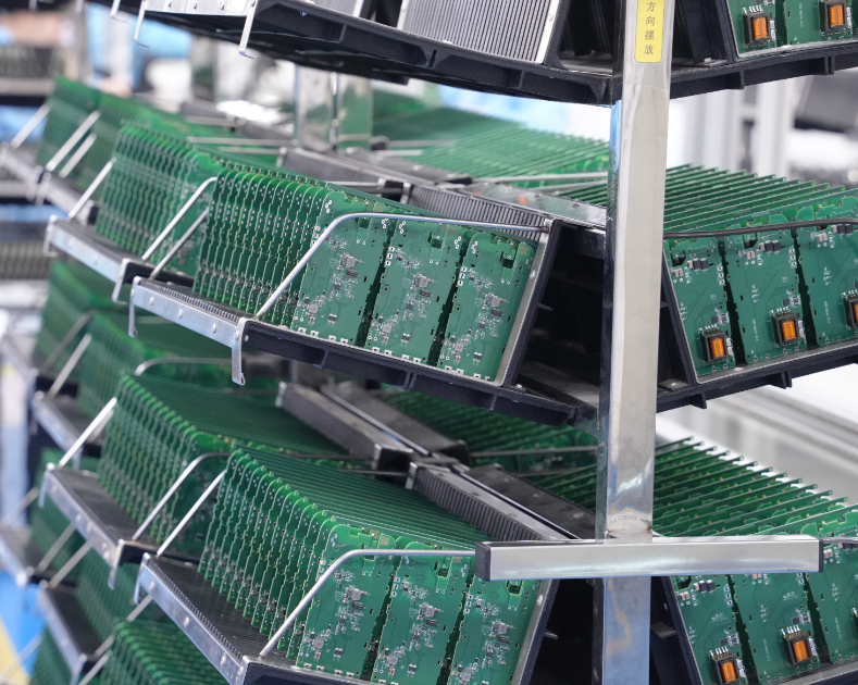
Benewave's manufacturing workflow includes automated SMT placement and inline inspection systems. These process controls can help identify assembly issues, but the specific inspection coverage should be agreed upon for each project.
Accurate placement alone does not guarantee a reliable solder joint. The solder paste stencil, aperture dimensions, paste properties, PCB pad geometry, and reflow profile must work together.
Very small components may be affected by excess solder, uneven paste deposits, or differences in wetting between pads. Larger components can introduce different challenges because of thermal mass and uneven heating.
For dense boards, solder paste inspection (SPI) can help detect deposition problems before they lead to placement or soldering defects. AOI can then identify many visible post-reflow defects, while X-ray may be needed for hidden joints such as those beneath BGAs.
Component placement limits are also influenced by the board itself. A component may be within the machine's supported size range but still be difficult to assemble if it is too close to a board edge, neighboring component, fixture, or tall part.
A design-for-manufacturing (DFM) review should check:
Component footprints against manufacturer datasheets.
Pad dimensions and pitch.
Clearance between adjacent components.
Board fiducial placement and visibility.
Tall-part interference and nozzle access.
Panelization, board support, and deformation risks.
Access for AOI, X-ray, electrical testing, and rework.
These checks are particularly important when moving from a working prototype to repeatable mass production.
Before approving a supplier, ask for specific answers instead of relying on general claims such as “high-precision SMT.”
What is the smallest package supported? Confirm whether the line can handle your actual 01005 or 0201 components, including the required feeder and nozzle configuration.
Which fine-pitch packages are supported? Provide the BGA, QFN, CSP, or WLCSP package dimensions and pitch for review.
How are large or irregular components handled? Ask whether automatic placement, tray feeding, manual placement, or DIP assembly is appropriate.
What inspection methods are available? Determine whether SPI, AOI, X-ray, ICT, or functional testing is required for the board.
Can the supplier support both prototypes and volume production? Confirm that process settings, inspection criteria, and component sourcing can remain controlled as order quantities increase.
Benewave offers integrated PCB fabrication, component sourcing, SMT and DIP assembly, programming, testing, and box-build services. Coordinating these stages can help buyers identify component-handling or test-access issues earlier, rather than discovering them after parts have been purchased or boards have entered production.
No. The ability to place 01005 components depends on the machine, feeder, nozzle, vision system, PCB layout, and process controls. Buyers should confirm capability for the exact package and production conditions.
No. Larger components may be easier to see, but their weight, shape, height, packaging, and required mounting method can make them difficult to handle. Some parts need specialized equipment or through-hole assembly.
There is no single accuracy requirement for all fine-pitch packages. The necessary capability depends on lead or ball pitch, pad geometry, package design, PCB tolerances, and the equipment specification. Ask the supplier to evaluate the actual footprint and component datasheet.
No. AOI checks visible features and can detect many placement and soldering defects, but it cannot directly inspect every hidden joint. BGA and other concealed connections may require X-ray inspection or additional electrical testing.
Provide the BOM, Gerber files, pick-and-place or centroid data, assembly drawings, component datasheets for unusual packages, and any inspection or functional-test requirements. These details help the manufacturer evaluate whether the proposed line and process are suitable.
If your project includes 01005 passives, fine-pitch ICs, BGAs, or large and irregular components, contact Benewave at zoe@benewavetech.com to review your PCB files, component list, and production targets. Benewave can help assess SMT and DIP assembly requirements, inspection coverage, and the manufacturing route for your prototype or mass-production order.
Find Partners, Not Just Suppliers
Expert OEM & PCBA manufacturing tailored to your exact specifications. Contact us today to discuss your project and discover a more collaborative way to manufacture.
Get a Fast Quote & Free DFM Review
Related PCB Assembly Service