Phone: +86-137 5102 2384
Phone: +86-137 5102 2384
Oct. 19, 2026
Share:
Choosing between SMT vs through-hole assembly for high-reliability PCB is rarely a simple cost decision. Engineers comparing the best PCB assembly method for mixed-technology boards must balance board area, mechanical stress, thermal performance, production volume, and repairability. Surface-mount technology uses reflow soldering and automated pick-and-place equipment, while plated through-hole assembly commonly uses wave soldering or selective soldering. This guide explains the practical difference between SMT and through-hole PCB assembly, including pricing, reliability, manufacturing limits, and real-world selection examples.

A PCB may work correctly in the laboratory and still fail after six months in the field. The failure may come from vibration loosening a connector, repeated thermal cycling cracking a solder joint, or a large through-hole component occupying routing space needed for power and signal layers.
At the same time, choosing SMT for every component is not automatically the best decision. A 10-pin, 2.54 mm connector that receives repeated insertion force may be more dependable with through-hole anchors. A high-volume control board containing 0201 resistors, QFNs, and fine-pitch ICs may become unnecessarily expensive if most of its components are manually inserted.
The most common questions from designers are:
In practice, the answer is often a mixed-technology PCB assembly rather than an absolute choice between two processes.
| Parameter | SMT Assembly | Through-Hole Assembly |
|---|---|---|
| Component placement | Components are placed directly on PCB pads. | Leads pass through drilled holes and are soldered to pads. |
| Typical solder process | Reflow soldering using solder paste and a controlled thermal profile. | Wave soldering, selective soldering, or manual soldering. |
| Board density | High density; supports small packages such as 0402, 0201, QFN, and BGA. | Lower density because drilled holes consume routing area and restrict layer transitions. |
| Automation potential | Usually highly automated through stencil printing, SPI, pick-and-place, and AOI. | Automatic insertion is possible, but many parts still require selective or manual insertion. |
| Mechanical strength | Good for most electronic components, but connectors and heavy parts may need reinforcement. | Excellent mechanical anchoring because leads pass through the PCB. |
| Prototype flexibility | Good when components are available and stencil or dispensing costs are acceptable. | Convenient for hand assembly, wire connections, and large leaded components. |
| Thermal management | Exposed copper areas and thermal vias can transfer heat efficiently, especially beneath power packages. | Large leads and copper planes can provide strong thermal paths, although drilling and solder filling must be controlled. |
| Inspection | AOI and X-ray inspection are commonly used for hidden joints such as BGAs and bottom-terminated components. | Visual inspection is often easier, although hidden barrel or underside defects may still require additional testing. |
| Board cost at medium and high volume | Often lower per unit because placement is fast and labor content is reduced. | Can cost more when insertion, soldering, and inspection require multiple process steps. |
| Repairability | Requires trained hot-air, micro-soldering, or rework equipment for fine-pitch devices. | Generally easier to remove and replace with conventional soldering tools. |
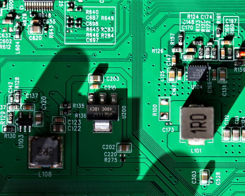
SMT is usually preferred when the design requires a small enclosure, short signal paths, or a high component count. A 100 mm × 80 mm board containing several hundred resistors, capacitors, microcontrollers, memory devices, and sensors can often be routed more efficiently with SMT because components do not require a hole through every signal layer.
Modern SMT lines can place thousands of components per hour, although actual output depends on feeder setup, package mix, board size, nozzle changes, inspection requirements, and line balancing. A board populated mostly with 0402 or 0603 passives may have a much higher placement efficiency than a board containing many connectors and irregular mechanical parts.
SMT also supports double-sided assembly. Components can be mounted on both sides of a PCB, reducing board area. However, bottom-side component weight, component clearance, reflow temperature limits, and second-pass soldering must be reviewed during design for manufacturing.
Through-hole assembly remains valuable when a component experiences insertion force, cable tension, vibration, shock, or significant mass. Common examples include:
The through-hole lead creates a mechanical interlock with the PCB. This does not make every through-hole joint immune to failure, but it generally improves resistance to pull-out forces compared with a small surface pad. For connectors subjected to thousands of mating cycles, the mechanical design of the connector, mounting tabs, PCB thickness, solder fillet, and enclosure support is just as important as the assembly method.
There is no universal reliability winner. Reliability depends on joint geometry, solder alloy, copper balance, board material, thermal profile, component mass, operating temperature, vibration, and inspection quality.
For thermal cycling, the coefficient of thermal expansion mismatch between the component and PCB is a major factor. Leaded through-hole parts can absorb some movement through lead compliance. Rigid leadless SMT packages, such as ceramic capacitors and certain QFN packages, can experience higher solder-joint stress when the board repeatedly moves between low and high temperatures.
For mechanical loads, through-hole usually has an advantage. For electrical density and controlled production, SMT often has an advantage. IPC-A-610 acceptance criteria, IPC J-STD-001 soldering requirements, component qualification, and product-specific testing should be used instead of relying on the words “strong” or “weak.”
A reliable supplier should provide solder paste control, reflow or wave-solder profiles, AOI records, X-ray capability where appropriate, electrical testing, and traceability for materials and operators.
The cost of SMT and through-hole PCB assembly is determined by more than the component price. A realistic quotation may include tooling, stencil fabrication, programming, setup, feeder loading, placement, soldering, inspection, testing, rework allowance, and packaging.
| Cost factor | SMT effect | Through-hole effect |
|---|---|---|
| Initial setup | Stencil, machine programming, feeder setup, and first-article verification. | Insertion programming, fixtures, wave or selective-solder setup, and possible hand-work instructions. |
| Labor | Lower for repeatable, high-volume placement. | Higher when parts are inserted or soldered manually. |
| Low-volume prototypes | Setup may represent a large percentage of total cost. | Can be economical for small quantities with simple leaded components. |
| High-volume production | Usually benefits from automation and reduced touch labor. | Competitive when the design is optimized for wave or selective soldering. |
| Rework | Fine-pitch and BGA rework may require specialized equipment. | Individual joints are generally easier to access and repair. |
As a planning example, a 1,000-unit board populated with 400 mostly-SMT placements may be cheaper per unit than a board with only 80 components if the second design requires 60 manual through-hole insertions. Conversely, a board with 20 large connectors may cost less with a dedicated selective-solder process than with manual soldering of every connector.
Ask the assembler for a costed breakdown rather than comparing only the quoted unit price. The lowest price may exclude testing, conformal coating, programming, cable assembly, or the inspection level required by the end product.
Wearables, smart sensors, remote controls, and compact consumer products generally favor SMT. Small packages reduce board size, support automated double-sided assembly, and enable short electrical connections. Through-hole parts are usually limited to battery connectors, buttons, display connectors, or components that need mechanical reinforcement.
For a wearable operating from a small lithium-ion battery, design teams should also consider thermal exposure during reflow. Batteries, microphones, displays, and other heat-sensitive parts may need to be installed after reflow or connected through a separate assembly step.
Industrial controllers often use mixed technology. SMT handles microcontrollers, communication ICs, optocouplers, and passive networks. Through-hole parts may be selected for terminal blocks, relays, fuses, transformers, and field wiring.
In this environment, vibration testing, humidity testing, conformal coating compatibility, creepage distance, and serviceability may have greater influence than minimum board area. A connector that is easy to replace in the field can reduce maintenance downtime even if it increases assembly cost.
Automotive designs commonly combine SMT with through-hole or press-fit components. Engineers must consider temperature cycling, vibration, shock, humidity, chemical exposure, and long-term component availability. Large SMT components require careful board support and strain-relief design, while through-hole components require controlled hole fill and suitable soldering processes.
Automotive qualification is product-specific. Neither SMT nor through-hole alone guarantees compliance with AEC-Q requirements, PPAP documentation, or vehicle-level reliability targets.
Power designs may use both technologies. SMT MOSFETs, drivers, current-sense resistors, and thermal-pad packages can provide short current paths and efficient automated placement. Through-hole bus bars, high-current terminals, large inductors, and heavy capacitors can provide mechanical support and lower-resistance connections.
Designers should calculate current density, copper cross-section, temperature rise, creepage, clearance, and solder-joint heating. A through-hole lead is not automatically a low-resistance power path; the lead diameter, plating, solder coverage, and PCB copper structure must be verified.
Through-hole can be convenient for hand-built prototypes because component leads are easy to position and inspect. However, many modern ICs, sensors, and wireless modules are available only in SMT packages. For this reason, a prototype may use breakout boards or adapters initially, then move to direct SMT placement in the production revision.
For field-service products, through-hole may simplify repair, but repairability also depends on access, test points, component availability, conformal coating, and whether the board is designed as a replaceable module.
A representative industrial-control project involved a compact controller with a microcontroller, isolated communication interface, relay outputs, screw terminals, and a 24 VDC power section. The first prototype used through-hole components for nearly every part because the engineering team wanted easy manual assembly. The board required a larger outline, had limited routing space, and needed repeated manual soldering.
In the production revision, the design team moved the microcontroller, isolation devices, resistors, capacitors, and signal diodes to SMT. The relays, terminal blocks, transformer, and fuse remained through-hole. The result was a mixed-technology board with fewer manual insertion steps and stronger mechanical support at the field-wiring interface.
During pilot production, the team added selective soldering for the through-hole components and AOI after reflow. The key improvement was not simply a smaller PCB. It was a clearer process split: SMT parts were handled by automated placement and reflow, while mechanically demanding components received through-hole insertion and selective soldering. The customer also reported easier connector replacement during service because the high-stress terminals were not dependent on small surface pads.
This case illustrates a useful engineering principle: select the mounting technology according to the component’s electrical and mechanical role, not according to a desire to make the entire board “all SMT” or “all through-hole.”
When engineers evaluate PCB assembly suppliers, positive feedback usually focuses on measurable production behavior rather than marketing claims. Useful customer comments often mention:
Benewave can be considered when a project needs a coordinated one-stop PCB assembly service covering component sourcing, SMT, through-hole insertion, selective soldering, inspection, testing, and final assembly. The correct evaluation is still evidence-based: request sample inspection records, process capability information, certifications, production photos, and a pilot-build plan before committing to volume production.
SMT is generally the strongest starting point when the board contains fine-pitch processors, memory, sensors, RF modules, and hundreds of passive components. It is especially suitable when board area is constrained and annual production volume justifies automated setup.
Use through-hole for connectors, heavy transformers, relays, large inductors, terminal blocks, and components exposed to repeated external force. Verify hole fill, solder fillet, lead trimming, and board support during production validation.
A hybrid approach frequently provides the best engineering balance. Place electrically dense circuitry with SMT and mechanically demanding or high-mass components with through-hole. Plan the solder sequence early because through-hole parts can interfere with bottom-side SMT and wave-solder pallet design.
Manual insertion can be appropriate for a small prototype, engineering change, or repair. It becomes less attractive when the bill of materials contains many repeated parts, when production exceeds a few dozen or few hundred units, or when solder quality must be highly consistent between operators.
SMT is suitable for compact, high-density, automated PCB production, particularly when the design uses fine-pitch ICs and a large number of passive components. Through-hole is suitable for connectors, heavy components, field wiring, and applications exposed to mechanical stress. Mixed technology is often the most practical choice for industrial controls, power electronics, communication equipment, and products that combine dense electronics with rugged interfaces.
Designers should not select a process based only on the lowest quoted assembly price. Compare total landed cost, board area, inspection requirements, failure risk, serviceability, production volume, and component availability. A capable supplier such as Benewave can help convert the schematic and BOM into a manufacturable process plan, but the final decision should be supported by a DFM review and a pilot build.
For the best PCB assembly method for mixed-technology boards, evaluate SMT placement, through-hole insertion, reflow soldering, wave soldering, and IPC-A-610 acceptance criteria together. If your design includes high-density circuitry and mechanically stressed interfaces, request a one-stop PCB assembly review before releasing the next PCB revision.
Yes. Mixed-technology assembly is common. SMT components may be assembled by reflow first, followed by through-hole insertion and wave, selective, or manual soldering. The sequence depends on component orientation, board layout, solder-side clearance, and thermal constraints.
Through-hole generally offers stronger mechanical anchoring, especially for connectors and heavy components. SMT can provide excellent electrical and thermal reliability when the footprint, solder profile, board support, and inspection process are properly controlled. Reliability depends on the application and manufacturing quality.
At medium and high volume, SMT is often cheaper per placement because the process is highly automated. Through-hole may be economical for a small number of large components or low-volume prototypes. The correct comparison must include setup, labor, tooling, inspection, soldering, and rework.
Through-hole is often preferred when the connector receives repeated mating force, cable pull, vibration, or side loading. Surface-mount connectors can also be reliable when they include mechanical hold-down tabs, solder anchors, or enclosure support.
Yes, but the design must use suitable copper thickness, thermal vias, wide conductors, appropriate packages, and controlled temperature rise. High-current terminals, bus bars, large inductors, and heavy capacitors may still benefit from through-hole or press-fit construction.
Most assemblers need Gerber or ODB++ files, a complete BOM with manufacturer part numbers, centroid data, PCB stack-up, assembly drawings, special process notes, testing requirements, and target quantity. Supplying approved alternates can reduce procurement delays.
Request a DFM and DFA review, verify the component lifecycle, build a pilot lot, inspect solder joints, run electrical and functional tests, and record defects by process step. A pilot build is more informative than relying only on a desktop prototype because it exposes stencil, feeder, soldering, and inspection issues.
Find Partners, Not Just Suppliers
Expert OEM & PCBA manufacturing tailored to your exact specifications. Contact us today to discuss your project and discover a more collaborative way to manufacture.
Get a Fast Quote & Free DFM Review
Related PCB Assembly Service