PCB Prototype Testing Checklist Before Starting Volume Production
Oct. 20, 2026
Share:
Summary: A reliable one stop pcb assembly partner can help coordinate fabrication, component sourcing, assembly, inspection, and testing, but the manufacturer should not be expected to discover every design or process weakness after production begins. This checklist explains how to validate a PCB prototype, document measurable acceptance criteria, confirm supplier capability, complete reliability testing, and authorize a controlled transition to volume production. It also provides a SERP-informed content map, practical testing steps, authoritative standards, and additional article ideas for engineers, purchasing teams, and contract manufacturers.
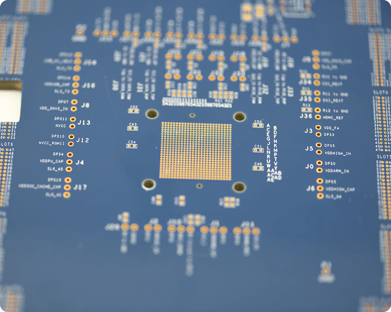
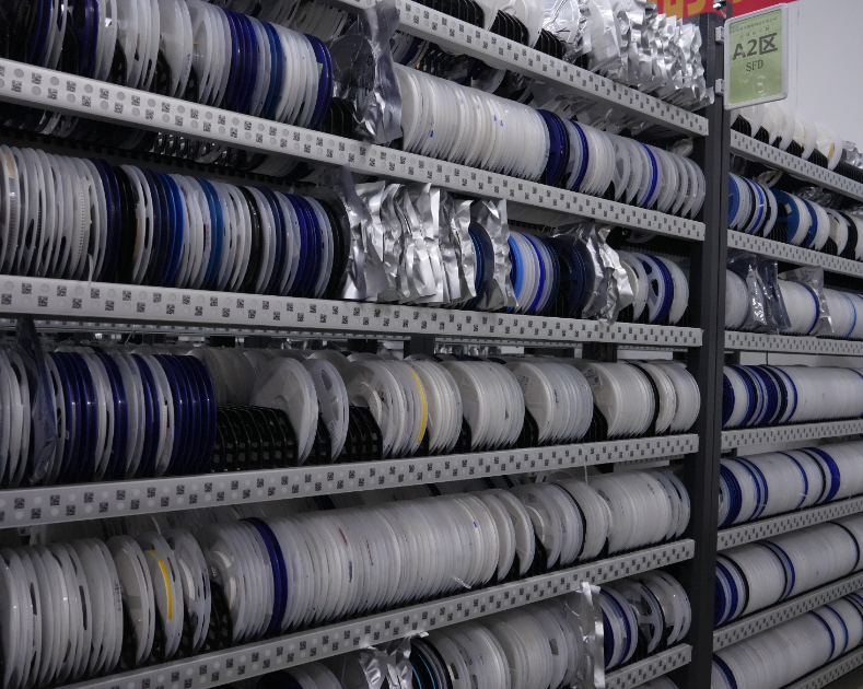
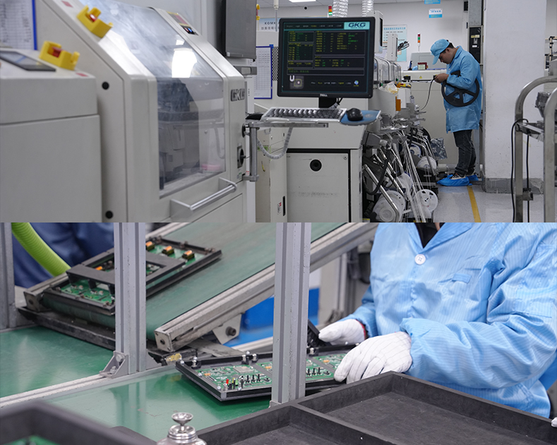
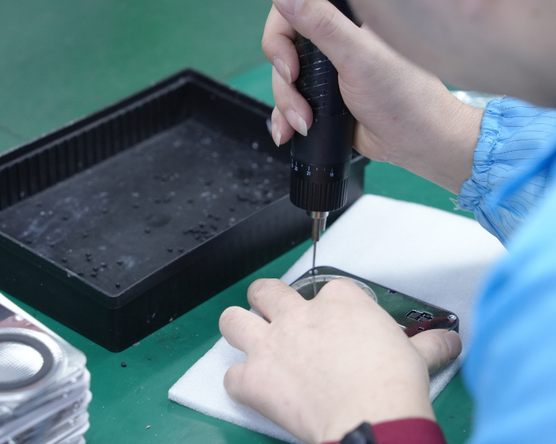
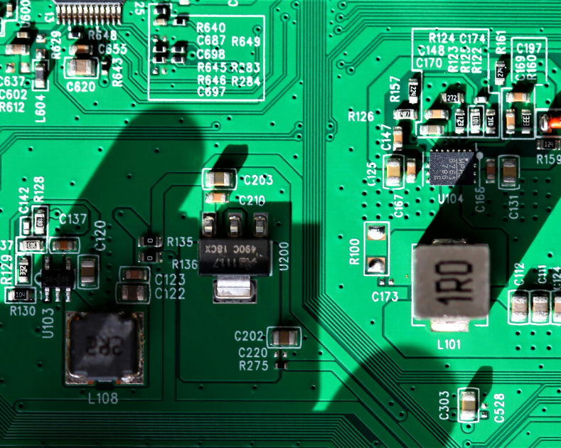
Benewave supports a structured PCB prototype-to-production workflow covering assembly, inspection, testing, and manufacturing readiness.
What the Search Results Commonly Focus On
Search results for “PCB Prototype Testing Checklist Before Starting Volume Production” generally reflect several overlapping search intents: preventing costly manufacturing defects, verifying electrical performance, preparing production documentation, and reducing the risk of field failure. Google rankings change by location, device, and time, so the following list is best used as a competitor-content and editorial planning snapshot rather than a permanent ranking claim.
Prototype manufacturing guides: Explain how to review Gerber files, drill files, stackups, materials, and design-for-manufacturing requirements before ordering.
PCB inspection checklists: Focus on visual inspection, automated optical inspection, X-ray inspection, solder-joint quality, and assembly workmanship.
Contract-manufacturing transition guides: Recommend a pilot run, golden sample, first-article inspection, process capability review, and formal production release.
Test-engineering resources: Compare test coverage, fixture costs, test-point access, automated test equipment, and debugging efficiency.
Prototype-to-volume case studies: Highlight how early supplier involvement, documented revisions, and closed-loop corrective action reduce production delays.
Six Actionable Article Outline Ideas for Related PCB Manufacturing Content
1. PCB Design-for-Manufacturing Checklist for First-Time Hardware Teams
Compare the design against the chosen fabricator’s minimum capabilities.
Check panelization, fiducials, tooling holes, assembly orientation, and depanelization risks.
Explain how DFM feedback affects yield and unit cost.
2. Flying-Probe Testing vs. ICT for PCB Prototype and Pilot Runs
Explain the operating principles of each test method.
Compare fixture investment, setup time, coverage, and debugging speed.
Identify when a prototype should move from flying-probe testing to a dedicated ICT fixture.
Include a decision matrix for low-, medium-, and high-volume programs.
3. How to Build a PCB First-Article Inspection Report
List required documents, dimensional checks, material certifications, and inspection results.
Show how to compare the assembled board with the approved bill of materials and drawings.
Explain nonconformance classification and corrective-action approval.
Provide a first-article acceptance template.
4. PCB Reliability Testing for Harsh Industrial and Automotive Environments
Cover thermal shock, temperature cycling, humidity, vibration, shock, and corrosion testing.
Link test conditions to the real operating environment.
Explain sample size, test duration, failure criteria, and post-test inspection.
Discuss conformal coating and enclosure-level validation.
5. Component Risk Management Before PCB Volume Production
Review lifecycle status, lead time, approved vendors, and counterfeit risk.
Define rules for substitutions and engineering-change approval.
Explain moisture-sensitive device handling, floor life, and baking requirements.
Build a supply-chain risk scorecard for every critical component.
6. PCB Assembly Yield Improvement: From Prototype Defects to Stable Production
Classify defects by design, material, equipment, process, and operator cause.
Use Pareto analysis to prioritize corrective actions.
Measure first-pass yield, rework rate, defects per million opportunities, and test escape rate.
Show how a pilot build validates process capability before volume release.
Why Prototype Testing Must Be Completed Before Volume Production
A prototype proves that a design can be built and operated under limited conditions. It does not automatically prove that the same design can be manufactured repeatedly, tested efficiently, sourced reliably, or survive its intended service environment.
Prototype quantity is usually too small to expose process variation: A single successful board may hide stencil, placement, soldering, or material problems.
Engineering samples may use temporary workarounds: Hand-soldered wires, modified components, bodge wires, or manual programming can conceal production barriers.
Volume production magnifies small defects: A 2% defect rate may be manageable during a ten-board prototype but unacceptable across 10,000 units.
Late changes are expensive: Correcting a footprint or test-access problem after tooling and inventory commitments can create scrap, delays, and regulatory complications.
Testing must match the product risk: A consumer indicator board may need basic functional testing, while a medical, automotive, aerospace, or industrial-control board may require documented reliability and traceability evidence.
Step 1: Freeze and Control the PCB Prototype Design
Do not begin formal testing with an uncontrolled design revision. Establish a clear baseline so that every test result can be traced to the exact hardware and software configuration used.
Assign a unique revision number to the schematic, PCB layout, bill of materials, firmware, drawings, and test procedure.
Archive the manufacturing data package, including Gerber or ODB++ files, Excellon drill files, pick-and-place files, assembly drawings, and fabrication notes.
Confirm that the bill of materials includes manufacturer part numbers, approved alternates, lifecycle status, tolerances, package types, and sourcing restrictions.
Record all engineering changes made during prototype assembly, including wire modifications, component substitutions, rework, and firmware patches.
Mark each prototype with a serial number or lot identifier.
Define which changes require a new verification cycle and which changes can be handled through documented deviation approval.
Use a configuration-management system or controlled document repository rather than relying on email attachments. The objective is to make it impossible for the manufacturer, test engineer, and purchasing team to work from different revisions.
Step 2: Complete a PCB Design-for-Manufacturing and Design-for-Assembly Review
Conduct a formal DFM and DFA review with the fabricator and assembly supplier before releasing the pilot build.
Confirm minimum trace width, spacing, hole diameter, annular ring, copper-to-edge clearance, and solder-mask dam capability with the fabricator.
Check whether high-current paths have adequate copper area, thermal relief, via capacity, and temperature-rise performance.
Review differential-pair routing, return paths, reference planes, via transitions, and impedance coupons for high-speed interfaces.
Confirm that plated slots, castellations, edge contacts, back drilling, buried vias, or sequential lamination requirements are clearly documented.
Inspect copper balance and panel utilization to reduce warpage and improve manufacturing efficiency.
Review the assembly design
Check component-to-component spacing and clearance from the PCB edge.
Confirm that polarized components, pin 1 indicators, reference designators, and polarity marks are visible after assembly.
Ensure all surface-mount parts have suitable land patterns and solder-mask openings.
Review thermal pads, via-in-pad structures, solder-paste apertures, and voiding risks.
Confirm that tall, heavy, heat-sensitive, or mechanically fragile components can be assembled in the intended sequence.
Provide fiducials, tooling holes, barcode locations, and test points suitable for automated equipment.
IPC-2221 provides generic printed-board design guidance, while IPC-A-610 and IPC-J-STD-001 are commonly used references for assembly acceptability and soldering requirements. The exact acceptance class should be selected according to product risk and customer requirements.
Step 3: Verify the PCB Fabrication and Material Package
Before evaluating assembly performance, verify that the bare board itself matches the approved construction.
Check finished board dimensions, thickness, flatness, bow, twist, and routed or scored edge quality.
Verify plated-through hole quality, hole-wall copper thickness, pad adhesion, surface finish, and solderability.
Inspect solder mask for registration, coverage, pinholes, bubbles, exposed copper, and contamination.
Check silkscreen readability, barcode quality, polarity marks, and revision information.
Review the fabricator’s certificate of conformance and material certificates.
Request microsection data when the application requires documented via and plated-hole quality.
Use impedance-test results or coupons when controlled impedance is part of the design requirement.
For rigid and rigid-flex boards, IPC-6012 and related IPC performance specifications can help define fabrication expectations. The supplier should state which revision and acceptance criteria are being applied.
Step 4: Inspect Assembly Workmanship Before Applying Power
Power should not be applied to an unverified prototype. Start with non-destructive inspection and compare the board against the approved assembly data.
Confirm the correct PCB revision, component population, and assembly orientation.
Check for missing, wrong, shifted, tombstoned, skewed, lifted, damaged, or incorrectly polarized components.
Inspect solder joints for bridges, insufficient solder, dewetting, non-wetting, excessive solder, voiding, and disturbed joints.
Check connectors, switches, shields, heat sinks, and mechanically stressed components for secure attachment.
Inspect reflowed and wave-soldered areas separately because their defect patterns and acceptance criteria differ.
Use magnification appropriate to package size and risk.
Record photographs of defects and link every defect to a board serial number.
Use the correct inspection technology
Visual inspection: Useful for markings, polarity, mechanical damage, and obvious solder defects.
Automated optical inspection: Effective for component presence, placement, polarity, solder fillets, and many visible assembly defects.
Automated X-ray inspection: Valuable for bottom-terminated components, hidden solder joints, BGA packages, and internal voiding.
Microscopy: Appropriate for fine-pitch packages, solder-mask clearance, wire modifications, and suspected cracks.
Cross-section or microsection analysis: Used when plated-hole, via, laminate, or solder-joint construction must be examined destructively.
Step 5: Perform Bare-Board Electrical Testing
Test the fabricated PCB before components are installed whenever practical. This separates board-manufacturing defects from assembly and component defects.
Perform continuity testing on required nets.
Perform isolation testing between nets according to the design and safety requirements.
Check for unintended shorts between power rails and ground.
Verify plated-through holes and via connections on critical nets.
Confirm controlled-impedance results where required.
Record the test voltage, resistance threshold, test method, equipment identification, and result.
Require a certificate of electrical test for production lots when appropriate.
Flying-probe testing is often practical for prototypes and low-volume builds because it avoids a dedicated fixture. A fixture-based test may become more economical and faster when production volume, test coverage, or cycle-time requirements increase.
Step 6: Create a Power-Up and Electrical Bring-Up Procedure
Use a controlled bring-up process rather than connecting an unverified prototype directly to a full-power supply.
Inspect the board for shorts, incorrect polarity, foreign material, and unpopulated safety-critical parts.
Use a current-limited bench supply for the first power application.
Power each rail independently when the design permits it.
Measure resistance to ground before power-up and compare it with the expected range.
Record inrush current, steady-state current, rail voltage, ripple, startup time, and shutdown behavior.
Verify power sequencing, reset behavior, clock startup, and supervisor operation.
Check regulators, converters, batteries, charging circuits, and protection devices for abnormal temperature.
Use an oscilloscope to inspect overshoot, undershoot, switching noise, clock quality, and transient response.
Document every deviation and link it to a corrective action or approved design change.
Step 7: Run In-Circuit, Functional, and Boundary-Scan Tests
In-circuit test checklist
Verify component presence and value where the test system supports it.
Measure resistance, capacitance, diode behavior, and transistor junctions.
Check open circuits, solder bridges, wrong-value resistors, and missing connections.
Test power-rail isolation and ground continuity.
Confirm access to critical test points and connector pins.
Functional test checklist
Program the correct firmware version and record the programming result.
Verify processor boot, memory access, communications, sensors, displays, indicators, relays, motors, and user interfaces.
Test normal operation, minimum and maximum input conditions, and defined fault conditions.
Check interfaces such as USB, Ethernet, CAN, RS-485, SPI, I2C, UART, wireless, or proprietary buses.
Measure output accuracy, response time, current consumption, and protective shutdown behavior.
Save automated test logs and connect them to the board serial number.
Boundary-scan checklist
Use boundary scan when dense digital devices limit physical probe access.
Confirm that the devices support the required boundary-scan architecture.
Develop interconnect, memory, and device-level tests appropriate to the board.
Define how boundary-scan results complement rather than replace functional testing.
Test coverage should be risk-based. A test that detects a manufacturing defect is not necessarily sufficient to prove product functionality, safety, cybersecurity, or long-term reliability.
Step 8: Validate Thermal, Mechanical, and Environmental Performance
Test conditions should represent the product’s actual installation, enclosure, duty cycle, storage environment, and expected service life.
Thermal testing: Measure component temperatures, PCB hot spots, enclosure temperatures, and thermal-interface performance under normal and worst-case loads.
Temperature cycling: Expose boards to repeated high and low temperatures to identify solder, via, laminate, and component failures.
Vibration testing: Examine connectors, heavy components, solder joints, and mechanical mounting points.
Mechanical shock testing: Apply the shock profile expected during shipping, installation, or operation.
Drop and handling tests: Use these for portable or consumer products when the use case requires them.
Burn-in: Operate boards under controlled conditions to expose early-life failures, but do not treat burn-in as a substitute for design validation.
Corrosion testing: Consider salt, industrial contaminants, or other exposure where the product environment justifies the test.
NASA workmanship standards, IEC environmental-test standards, automotive qualification standards, and customer-specific specifications may apply depending on the product. Select and document the applicable standard before testing begins instead of choosing conditions after a failure occurs.
Step 9: Verify EMC, Safety, and Regulatory Requirements
A PCB can pass functional testing and still fail certification. Begin compliance planning during the prototype stage.
Review electromagnetic-emissions risks, including clock harmonics, switching converters, cable interfaces, and enclosure openings.
Check immunity risks from electrostatic discharge, electrical fast transients, surge, radiated fields, and conducted disturbances.
Confirm the required flammability rating for PCB materials and enclosures.
Document restricted substances and material declarations for applicable markets.
Plan pre-compliance testing before formal laboratory certification.
Keep a compliance matrix that maps each requirement to a test, inspection, document, or certification record.
Useful references may include the U.S. Code of Federal Regulations for regulated products, the European Union RoHS and REACH frameworks, IEC 62368-1 for certain audio/video and information-technology equipment, and applicable UL requirements. Product-specific legal and certification advice should come from a qualified compliance professional.
Step 10: Confirm Component Authenticity and Supply-Chain Readiness
Prototype parts obtained through spot purchasing may not be suitable for volume production. Confirm that the approved supply chain can support both quantity and quality.
Purchase critical components through authorized or verified distribution channels.
Check manufacturer date codes, lot codes, country of origin, packaging, labeling, and certificates.
Review component lifecycle status and identify parts at risk of obsolescence.
Approve alternates only after electrical, mechanical, firmware, thermal, and compliance impact analysis.
Confirm component availability for the full production forecast, not just the pilot build.
Identify long-lead components and create an approved last-time-buy or redesign plan.
Use incoming inspection or laboratory authentication for high-risk, high-value, or safety-critical components.
Step 11: Build a Controlled Pilot Run
The pilot run should simulate volume production as closely as possible. Avoid hand assembly and special engineering treatment unless those methods will also be used in production.
Use the planned production line, stencil, solder paste, placement program, reflow profile, inspection program, and test fixtures.
Build enough units to expose process variation and support environmental, destructive, and functional testing.
Record line settings, operator instructions, material lots, equipment IDs, and process timestamps.
Measure first-pass yield before rework.
Classify defects by cause and location.
Calculate rework rate, scrap rate, test escape rate, and defect opportunities.
Review whether the assembly cycle time and test cycle time meet the production target.
Retain representative units as golden samples and reference boards.
Step 12: Establish Acceptance Criteria and Process Capability
Volume release should be based on predetermined limits, not subjective confidence.
Define electrical limits for every critical rail, signal, output, and protection function.
Define dimensional, visual, soldering, and mechanical acceptance criteria.
Set maximum allowable defect, rework, and scrap rates.
Use statistical process control for critical variables such as solder-paste deposition, component placement, reflow temperature, impedance, and test measurements.
Calculate process capability where sufficient data exists, using appropriate Cp, Cpk, Pp, or Ppk methods.
Investigate trends before they become out-of-specification failures.
Define escalation rules for repeated defects and supplier corrective action.
Quality decisions should consider both specification compliance and process stability. A process that barely meets the specification but shows a negative trend may not be ready for volume production.
Step 13: Complete a Formal Production-Readiness Review
Use a cross-functional gate review involving design engineering, manufacturing engineering, quality, purchasing, regulatory, service, and the assembly supplier.
Confirm that the schematic, PCB layout, BOM, firmware, drawings, and test programs are released.
Approve the manufacturing data package and revision-control process.
Review all prototype and pilot defects, corrective actions, and verification evidence.
Confirm that no open critical or major nonconformance remains without documented approval.
Approve the golden sample and reference photographs.
Confirm production tooling, fixtures, test equipment, spare parts, and maintenance plans.
Approve component sources, alternates, incoming inspection, and traceability requirements.
Review packaging, labeling, ESD controls, storage conditions, and shipping validation.
Confirm capacity, lead time, yield targets, and production ramp assumptions.
Obtain written sign-off from the responsible decision-makers.
PCB Prototype Testing Checklist Before Volume Production
Design revision, BOM, firmware, drawings, and manufacturing files are controlled.
DFM and DFA reviews are complete and documented.
PCB material, stackup, copper, finish, dimensions, and impedance are verified.
Bare boards passed continuity and isolation testing.
Assembly passed visual inspection, AOI, X-ray, or other required inspection.
Critical solder joints and hidden connections were verified.
Controlled power-up testing passed without abnormal current or temperature.
In-circuit, flying-probe, boundary-scan, or equivalent structural testing is complete.
Functional testing covers normal, boundary, and fault conditions.
Firmware programming and version control are verified.
Thermal, mechanical, vibration, humidity, and reliability tests are complete where required.
EMC and safety pre-compliance risks have been evaluated.
Component authenticity, lifecycle, availability, and alternates are approved.
Pilot-run yield and process capability meet targets.
Test records are linked to serial numbers or lot numbers.
Corrective actions are closed or formally accepted.
Production-readiness approval has been signed.
Key PCB Production Risks That Are Often Overlooked
Test-point access and fixture design
A board may be electrically correct but difficult or expensive to test. Reserve access for power rails, grounds, reset lines, programming interfaces, communication buses, and safety-critical signals. Confirm probe clearance, fixture orientation, board support, and operator safety before layout release.
Firmware, calibration, and test-data control
Define the approved firmware image, calibration constants, programming process, checksum method, and data-retention requirements. A production board should never leave the line with an untraceable software version or manually entered calibration value.
ESD and moisture controls
Specify ESD-protected workstations, grounding methods, packaging, humidity monitoring, and handling rules. For moisture-sensitive devices, document floor life, dry storage, baking, and exposure records.
Cleaning and ionic contamination
Flux residues and ionic contamination can cause leakage, corrosion, dendritic growth, and intermittent failures. Define whether the board will be cleaned, which chemistry will be used, and how cleanliness will be verified. Consider ionic cleanliness testing for high-impedance, high-voltage, or harsh-environment products.
Connector mating and mechanical integration
Test the PCB inside the final enclosure with the actual cables, connectors, fasteners, shields, thermal interfaces, and mounting torque. Problems often appear only after enclosure integration, including cable strain, insufficient clearance, grounding faults, and heat accumulation.
Repairability and field service
Define whether defective boards will be repaired, scrapped, returned to the supplier, or analyzed. Establish rework limits, approved tools, replacement rules, and reinspection requirements. Excessive rework can reduce long-term reliability even when the board passes final testing.
How Benewave Can Support a Prototype-to-Production Transition
Benewave can be positioned as a manufacturing partner for teams that need coordinated PCB fabrication, component sourcing, assembly, inspection, testing, and production support. When evaluating Benewave or another supplier, request evidence rather than relying only on a capability list.
Ask for the supplier’s standard DFM and DFA review process.
Confirm available assembly technologies, package-size limits, layer-count capability, and material options.
Request sample inspection reports, first-article formats, and traceability examples.
Review AOI, X-ray, flying-probe, ICT, functional-test, and programming capabilities.
Confirm how engineering changes, component substitutions, and nonconformances are approved.
Ask how the supplier controls ESD, moisture-sensitive components, solder paste, reflow profiles, and cleaning.
Define communication responsibilities, escalation contacts, lead times, and production-release gates.
A one-stop supplier can simplify coordination, but the customer should retain ownership of product requirements, acceptance criteria, change control, and final release decisions.
Recommended Documentation Package for Production Release
Released schematic and PCB layout files.
Approved bill of materials with manufacturer part numbers and alternates.
Fabrication drawing, stackup, impedance requirements, and material specifications.
Assembly drawing, polarity details, component height restrictions, and special-process notes.
Gerber, ODB++, drill, pick-and-place, stencil, and panelization files.
Inspection criteria based on the selected IPC class or customer specification.
Electrical, functional, programming, calibration, and firmware test procedures.
Golden sample photographs and approved reference units.
Reliability, EMC, safety, and regulatory test reports.
First-article inspection and pilot-run reports.
Defect log, root-cause analysis, corrective-action records, and deviation approvals.
Packaging, labeling, storage, shipping, and traceability instructions.
Production-readiness review approval and release date.
Authoritative References for PCB Testing and Manufacturing Quality
IPC — Industry standards and guidance for PCB design, fabrication, assembly, soldering, and acceptability.
NASA Technical Standards — Workmanship and reliability references for high-reliability applications.
Release a PCB design to volume production only when the product has demonstrated functional performance, the assembly process has demonstrated repeatable yield, the supply chain has been verified, and every critical requirement has objective evidence. If a requirement cannot be measured, inspected, tested, or documented, it is not yet ready to serve as a production-control criterion.
The most effective PCB prototype testing process is not a single inspection at the end of development. It is a controlled sequence: freeze the design, review manufacturability, verify the bare board, inspect assembly, test electrical performance, validate the environment, confirm compliance, run a realistic pilot build, and approve production using documented evidence.
Expert OEM & PCBA manufacturing tailored to your exact specifications. Contact us today to discuss your project and discover a more collaborative way to manufacture.

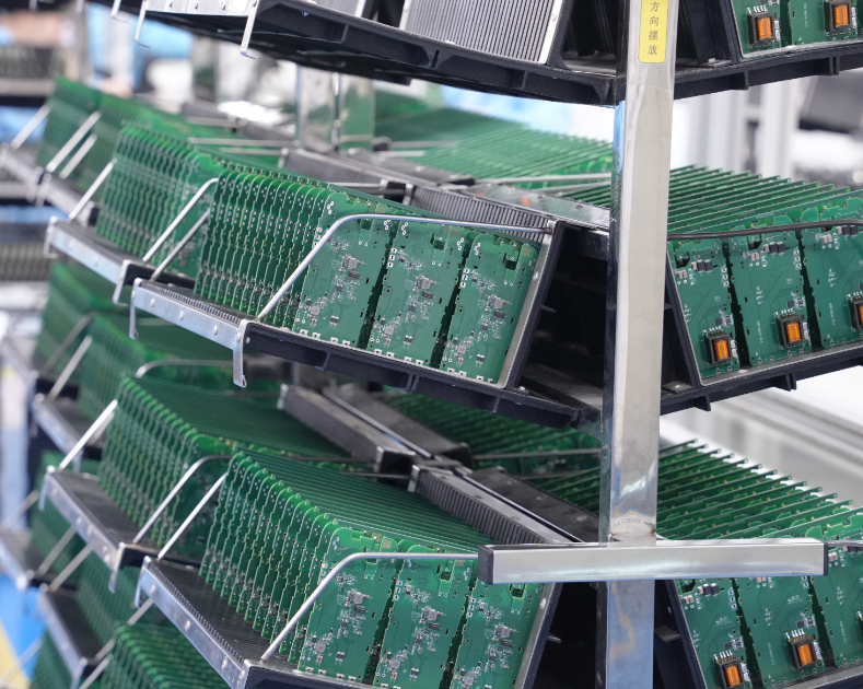
 Benewave supports a structured PCB prototype-to-production workflow covering assembly, inspection, testing, and manufacturing readiness.