
Phone: +86-137 5102 2384
Phone: +86-137 5102 2384
Jul. 14, 2026
Share:
In PCB assembly, automated optical inspection (AOI) and X-ray can verify that a component is present, correctly oriented, and properly soldered. But they cannot verify that the board actually works. A perfectly soldered BGA processor may contain a firmware corruption. A beautifully placed ADC may have an incorrect reference voltage due to a wrong resistor value that falls within tolerance but outside the design's sensitivity requirement. A pristine Ethernet PHY may fail to establish a link because of a subtle impedance mismatch in the differential pairs.
This is the domain of functional testing—the validation layer that confirms not just manufacturing correctness, but operational performance. In modern electronics manufacturing, functional testing is not a final gate to be passed before shipping. It is an integrated quality system that spans New Product Introduction (NPI), production ramp, volume manufacturing, and continuous improvement. When implemented strategically, it transforms test data from a pass/fail record into a predictive asset that drives process optimization and reduces total cost of quality.
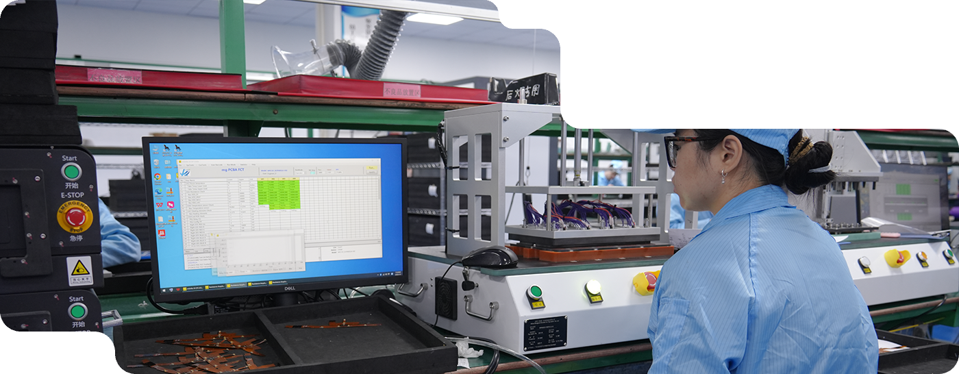
To understand functional testing's role, one must first understand what it is not. PCB assembly testing operates across three layers, each addressing a different fault spectrum:
Structural tests confirm that the board was built correctly, regardless of whether the design itself is correct.
In-Circuit Test (ICT): Uses a bed-of-nails fixture to access hundreds or thousands of test points simultaneously. ICT verifies component presence, orientation, and nominal value; detects solder opens, shorts, and wrong components; and can perform limited functional checks (e.g., verifying that an op-amp output swings correctly). It is fast (seconds per board) and highly effective for manufacturing defects but requires dedicated test fixtures and adequate test point coverage designed into the PCB.
Automated Optical Inspection (AOI) and X-Ray (AXI): While primarily inspection technologies, they serve a structural validation role by detecting missing components, solder defects, and polarity errors. They are non-contact and require no test points but cannot verify electrical performance.
Flying Probe Test: A fixtureless alternative to ICT where robotic probes move to test points on the PCB. It is ideal for prototypes and low-volume production where ICT fixture costs are prohibitive, but test times are significantly longer (minutes per board versus seconds).
Functional tests confirm that the assembled board performs its intended function under realistic electrical and environmental conditions.
Functional Circuit Test (FCT): Powers the board and exercises it through its operational modes. For a motor controller, FCT verifies PWM generation, current sensing accuracy, and overcurrent protection. For a communication module, it validates RF output power, frequency accuracy, and protocol conformance. FCT requires custom test fixtures, programmable power supplies, electronic loads, and often specialized instrumentation (spectrum analyzers, oscilloscopes, protocol analyzers).
Boundary Scan (IEEE 1149.1 JTAG): A structural-functional hybrid that accesses digital IC pins through a serial test port. It can detect opens and shorts on digital interconnects without physical probe access and can program flash memory and FPGAs. However, it requires JTAG-compatible devices and proper chain design during schematic capture.
Firmware Programming and Validation: Many modern PCBAs are inert without firmware. FCT includes bootloader programming, firmware flashing, MAC address assignment, calibration constant loading, and checksum verification. A board that passes ICT but fails firmware loading is a common NPI trap.
These tests validate that the board will survive its intended environment and operational life.
Burn-In: Powered operation at elevated temperature (typically 40–60°C above maximum rated ambient) for 48–168 hours to precipitate infant mortality failures in semiconductors.
Environmental Stress Screening (ESS): Thermal cycling and vibration applied to precipitate latent manufacturing defects (cold solder joints, delamination, cracked passives) without damaging good products.
Highly Accelerated Stress Test (HAST): 85°C/85% relative humidity with bias voltage to accelerate moisture-induced failures in poorly sealed or contaminated assemblies.
The most expensive mistake in PCB test strategy is assuming testability can be added after layout. DFT must be engineered during schematic capture and PCB layout:
ICT requires physical probe access to every net. Test points should be 0.8–1.0 mm diameter pads (or larger for high-volume fixtures) distributed across the board, not clustered under large components or at board edges where fixture sealing is difficult.
For high-density designs where test point real estate is scarce, prioritize nets with the highest manufacturing defect probability: power rails, clock lines, and analog feedback nodes.
Avoid placing test points on component pads unless using non-contact capacitive sensing; mechanical probing can damage solder joints or thin copper traces.
Digital ICs (processors, FPGAs, ASICs) should be connected into one or more JTAG chains with accessible TDI/TDO/TMS/TCK test ports.
Chain length should be limited (typically <8 devices) to maintain signal integrity and reduce test time.
JTAG cannot test analog circuits, power supplies, or memory interfaces that bypass the boundary scan cells. Complementary test access is required.
Complex systems-on-module (SoMs) and processors can incorporate BIST firmware that exercises memory, peripherals, and communication interfaces during power-up. BIST reduces external test equipment requirements but increases boot time and firmware complexity.
Large, complex boards should be designed with test isolation: power domains that can be enabled independently, communication buses that can be looped back, and analog sections that can be stimulated with on-board test signals. This allows FCT to localize faults without requiring exhaustive full-system test vectors.
During prototype and pilot builds, the test strategy prioritizes learning over throughput:
Flying probe or manual bench test: Used for first articles to validate design assumptions before investing in ICT fixtures.
Design Verification Test (DVT): Comprehensive functional testing under corner-case conditions (minimum/maximum input voltage, temperature extremes, load transients) to validate design margins.
Test program development: FCT software is developed and debugged in parallel with firmware, often revealing design issues (untestable states, race conditions, analog sensitivity) that require PCB respins.
As volume increases from hundreds to thousands of units, test strategy shifts toward automation and efficiency:
ICT fixture investment: Once design stability is confirmed, a bed-of-nails ICT fixture is fabricated. The fixture must be designed for durability—high-volume fixtures may execute 100,000+ actuations and require hardened probes and guided plates.
FCT fixture integration: Custom functional test fixtures integrate pogo-pin interfaces, RF shielded enclosures, thermal chambers, and automated handlers. Test time per board becomes a critical metric; a 5-minute FCT on a line producing 1000 units/day consumes 83 hours of capacity daily.
Test coverage validation: Correlation studies compare ICT/FCT results against AOI and field failure data to identify escape paths—defect types that slip through the test net.
At scale, the focus shifts to data-driven optimization:
Test time reduction: Parallel testing (testing multiple boards simultaneously), test sequence optimization (executing fastest tests first to fail bad boards early), and test compression (using BIST instead of external vectors) reduce cycle time.
Statistical Process Control (SPC): Test data—voltage readings, current consumption, frequency accuracy, temperature rise—is plotted on control charts. Trends toward specification limits trigger process audits before out-of-spec conditions produce failures.
Sampling strategies: For mature, stable products with low defect rates, 100% FCT may transition to sampling-based functional test (e.g., every 10th board) with 100% ICT retained for structural defect detection. This decision must be supported by statistical analysis of defect rates and field return data.
Testing is not free. A comprehensive ICT + FCT + burn-in regimen can add 10–30% to manufacturing cost. The optimal test strategy balances three variables:
Cost of Test (CoT): Fixture amortization, test equipment depreciation, labor, and test time.
Cost of Internal Failure (CoIF): Rework, scrap, and yield loss from defects caught at test.
Cost of External Failure (CoEF): Warranty claims, field service, brand damage, and liability from defects that escape to the customer.
The test investment is justified when:
CoT + CoIF < CoEF
For consumer electronics with low unit cost and replaceable products, minimal testing (AOI + sampling FCT) may be optimal. For automotive safety systems, medical devices, or aerospace avionics, where a single field failure can cost millions or endanger lives, exhaustive testing (100% ICT + 100% FCT + burn-in + ESS) is non-negotiable.
Modern test systems generate far more than go/no-go results. A fully instrumented FCT station may record hundreds of parametric measurements per board: power supply ripple, ADC offset, clock jitter, RF power, temperature rise, and communication bit-error rate. This data, when aggregated across thousands or millions of units, becomes a powerful quality intelligence asset:
If the mean value of a 3.3V regulator output gradually shifts from 3.30V to 3.28V over a production week, the board may still pass the 3.20–3.40V test limit. But the trend signals impending process drift—perhaps a reflow oven zone degrading, a solder paste batch changing, or a component lot approaching its tolerance edge. SPC control charts (X-bar, R-chart, Cpk tracking) flag these trends for preventive action before failures occur.
By correlating test measurements with component lot numbers, manufacturers can identify subtle parametric shifts caused by supplier process changes. A specific reel of 1% resistors that consistently produces ADC readings 0.5% low may be within tolerance individually but systematically degrading system accuracy when combined with other tolerances in the signal chain.
Machine learning models trained on test data can identify boards that pass all test limits but exhibit parametric signatures correlated with future field failures. For example, boards with elevated quiescent current consumption and slightly reduced clock amplitude—both within spec—may have a 10× higher probability of failing within the first year due to a marginal solder joint or near-defective component. These boards can be flagged for enhanced screening or rejected preventively.
Test data feeds back into the manufacturing process in real time:
SPI (Solder Paste Inspection) data showing trending paste volume reduction triggers automatic stencil cleaning or squeegee replacement.
ICT data revealing a cluster of capacitor value failures from a specific feeder slot triggers feeder maintenance before the defect spreads.
FCT data showing RF power degradation after a reflow oven maintenance event triggers immediate oven re-qualification.
100% ICT and FCT for safety-critical assemblies (ASIL-rated).
FCT includes fault injection (e.g., verifying that an overcurrent protection circuit trips within specification).
Full parametric data logging and traceability per board serial number for potential recall analysis.
Environmental testing (thermal cycling, vibration) as part of PPAP (Production Part Approval Process).
Process validation (IQ/OQ/PQ) for all test equipment and procedures.
FCT must verify patient isolation, leakage current, and safety interlock functionality for patient-contacting devices.
Calibration verification of all test instrumentation with NIST-traceable standards.
Full device history records (DHR) linking test results to component lots and operators.
100% ICT, FCT, and X-ray inspection for Class 3 assemblies.
ESS (thermal cycling and vibration) on 100% of flight hardware.
Burn-in for 168+ hours on critical assemblies.
Test data retained for the operational lifetime of the aircraft or system.
FCT includes protocol conformance testing (Ethernet RFC 2544, PCIe link training, SERDES eye diagram analysis).
Long-duration stress tests (24–72 hours of continuous traffic) to detect thermal-induced timing failures.
EMC pre-compliance testing as part of FCT for products with integrated radios.
Functional testing in PCB assembly quality control is far more than a final shipping gate. It is a multi-layered technical discipline that begins with Design for Testability during schematic capture, extends through structural and functional validation during production, and culminates in data-driven continuous improvement. The distinction between a good manufacturer and an excellent one often lies not in the presence of a test station, but in the sophistication of the test strategy, the depth of parametric data collection, and the speed with which that data is converted into process intelligence.
As products become more complex—integrating heterogeneous processors, high-speed interfaces, RF subsystems, and safety-critical functions—the test challenge grows exponentially. The manufacturers that thrive will be those that treat testing not as a cost center to be minimized, but as a strategic capability that protects brand reputation, reduces total cost of quality, and generates the data necessary to build ever-more-reliable products.
ICT (In-Circuit Test) is a structural test that verifies manufacturing correctness: component presence, orientation, value, and solder joint integrity. It uses a bed-of-nails fixture and is extremely fast but requires physical test point access. FCT (Functional Circuit Test) verifies that the board performs its intended function: power sequencing, signal processing, communication, and analog performance. It requires the board to be powered and exercised through operational modes.
You need both because they detect different defect types. ICT catches solder opens, shorts, wrong components, and missing parts—manufacturing defects that FCT may or may not detect depending on circuit topology. FCT catches design-margin issues, firmware errors, timing problems, and parametric drift that ICT cannot see. For high-reliability products, 100% ICT followed by 100% FCT is standard. For cost-sensitive consumer products, AOI plus sampling FCT may suffice.
Flying probe is ideal for prototypes, low-volume production (<500 units), and high-mix environments where dedicated ICT fixtures are economically unjustified. It requires no fixture investment and can be reprogrammed quickly for design changes. However, test times are 5–10× longer than ICT (minutes vs. seconds), making it unsuitable for high-volume lines. Additionally, flying probes cannot apply power to the board for active functional tests; they are limited to passive component measurement and continuity checks. The typical migration path is: flying probe for NPI → ICT fixture for volume production.
DFT is the practice of designing PCBs to be testable during manufacturing. It includes: (1) Test point placement—distributing accessible probe pads for ICT; (2) JTAG chain design—connecting digital ICs into boundary scan paths; (3) Test isolation—enabling power domains and buses to be tested independently; and (4) Built-in self-test (BIST)—embedding firmware diagnostics. DFT matters because testability cannot be added after layout without respinning the board. A PCB with no test points and no JTAG access may require 100% manual bench testing, increasing test cost by 10× and reducing coverage.
Test coverage should be driven by a risk-based approach: (1) Safety criticality—medical, automotive, and aerospace demand near-100% structural and functional coverage; (2) Field failure cost—high warranty or liability costs justify exhaustive testing; (3) Defect history—mature products with stable processes can reduce test intensity; (4) Component complexity—boards with fine-pitch BGAs, high-layer counts, or mixed technology require more comprehensive testing; and (5) Customer requirements—many OEMs mandate specific test regimes in their supplier quality agreements. A formal test coverage analysis should map each potential defect mode to a detection method and quantify residual risk.
Yes, when analyzed at scale. While a single board passing all test limits provides limited predictive information, population-level statistical analysis reveals subtle correlations. For example, boards with quiescent current in the top 5% of the distribution and clock jitter in the top 10%—both within specification—may show a 5–10× higher field failure rate due to marginal components or solder joints. Machine learning models trained on historical test data and field return data can identify these "gray zone" boards and flag them for enhanced screening or rejection. This transforms test data from a quality gate into a predictive quality intelligence system.
Find Partners, Not Just Suppliers
Expert OEM & PCBA manufacturing tailored to your exact specifications. Contact us today to discuss your project and discover a more collaborative way to manufacture.
Get a Fast Quote & Free DFM Review
Related PCB Assembly Service







