How to Build a PCBA Test Plan Before Mass Production
Oct. 20, 2026
Share:
A one stop pcb assembly project needs more than a good board design. Before mass production, the purchasing, engineering, and quality teams need a practical PCBA test plan that defines what will be tested, how it will be tested, which equipment is required, and how results will be approved. This guide explains how to create that plan step by step, control testing costs, reduce production risk, and choose a manufacturing partner such as Benewave.
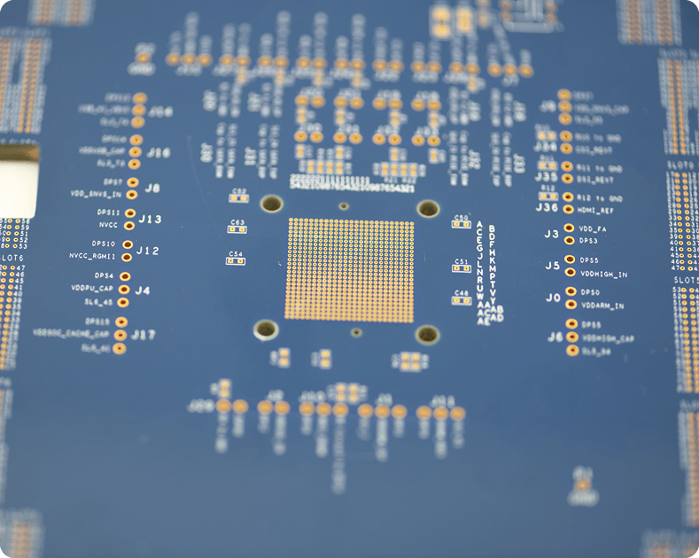
A complete PCBA test plan connects design requirements, test coverage, equipment, quality records, and mass production control.
Purchasing teams typically want more than a general explanation of ICT, flying probe testing, or functional testing. They need a clear plan that helps them compare supplier quotations, identify hidden test costs, confirm delivery risks, and prevent defective PCB assemblies from reaching customers.
1. Define the Test Plan Goals and Production Scope
Start with the product requirements
The first step is to define why the PCBA will be tested and what the test process must prove. A test plan should connect every test item to a product requirement, drawing note, electrical specification, safety requirement, or customer expectation.
Identify the PCBA model, revision, and target production volume.
Define the intended product application and operating environment.
List all critical electrical, mechanical, software, and safety requirements.
Identify the acceptable performance range for each requirement.
Define the expected production yield and maximum defect rate.
Specify whether testing is required at prototype, pilot, mass production, or every stage.
Set clear test objectives
Typical PCBA test objectives include confirming component presence, checking solder quality, verifying electrical connections, validating firmware, detecting assembly defects, and proving that the board performs its intended function.
Detect open circuits, short circuits, and incorrect component values.
Confirm the correct component part number and orientation.
Verify power rails, current consumption, and signal levels.
Check communication interfaces such as USB, CAN, UART, SPI, I2C, Ethernet, or RS485.
Validate sensors, displays, motors, relays, LEDs, and other functional outputs.
Confirm firmware programming and version control.
Record test results for traceability and customer audits.
Define the production stages that require testing
Testing only at the end of assembly can allow defects to move through several process steps. A stronger plan assigns tests to the points where defects can be found most efficiently.
Incoming inspection for bare PCBs, components, and programmed devices.
Post-assembly inspection after SMT and through-hole soldering.
Automated optical inspection after solder paste printing and component placement.
In-circuit testing after assembly and before final functional testing.
Firmware programming and software verification.
Functional testing under normal and abnormal operating conditions.
Final inspection, labeling, packaging, and shipment release.
2. Convert Design Requirements into Testable Items
Create a requirement and test coverage matrix
The second step is to convert design information into a test matrix. This matrix prevents important requirements from being overlooked and gives purchasing teams a precise document for supplier comparison.
Requirement
Test method
Acceptance criteria
Test stage
Record required
Input voltage
Power supply measurement
Within specified voltage range
Functional test
Yes
Short circuit protection
Controlled overload test
No unsafe temperature rise or damage
Engineering validation
Yes
Component value
In-circuit test or automated measurement
Within component tolerance
ICT
Yes
Communication interface
Protocol communication test
Correct data transmission and response
Functional test
Yes
Firmware version
Programming and software verification
Approved firmware checksum
Programming station
Yes
Classify test items by risk
Not every test has the same importance. Classifying test items by risk helps the team spend time and money on the characteristics that can cause safety failures, field returns, or major production losses.
Critical items: safety circuits, power inputs, high-current paths, insulation, protection functions, and components that can cause product damage.
Major items: communication interfaces, sensors, processors, memory, analog accuracy, and output control.
Minor items: cosmetic indicators, non-critical labels, and features that do not affect basic operation.
Identify design-for-test requirements
Test coverage depends heavily on the PCB layout. Review the design before production tooling begins. Test points, access areas, programming connectors, and fixture clearance are difficult and expensive to add after the board is released.
Add accessible test points for power, ground, clocks, reset lines, and communication signals.
Provide sufficient spacing for probe access.
Include programming and debug connectors where needed.
Mark polarity, pin one, and connector orientation clearly.
Keep test points away from tall components and mechanical obstructions.
Provide a stable method for grounding the unit during testing.
Review whether sensitive circuits need guarded or isolated measurements.
3. Select the Right PCBA Test Methods
Compare the main test methods
The third step is to select one or more test methods based on board complexity, production volume, access requirements, defect risk, and budget. No single method provides complete coverage for every PCBA.
Test method
Best use
Main advantages
Main limitations
Visual inspection
Basic assembly and marking checks
Low cost and fast
Cannot verify hidden or electrical defects
Automated optical inspection
Solder joints and component placement
Fast repeatable inspection with image records
Limited for electrical performance and hidden joints
X-ray inspection
BGA, QFN, bottom-terminated, and hidden solder joints
Can inspect concealed connections
Higher cost and slower throughput
In-circuit testing
Component values, shorts, opens, and nodes
Good coverage for high-volume production
Requires test points and fixture investment
Flying probe testing
Low-volume or frequently changing products
Low fixture cost and flexible programming
Slower cycle time than a dedicated ICT fixture
Functional testing
Complete product behavior and system operation
Confirms real operating performance
Requires custom hardware, software, and procedures
Burn-in or stress testing
Products exposed to long operation or harsh conditions
Can reveal early-life failures
Increases cycle time and energy cost
Choose testing based on volume and product risk
For low-volume products with frequent design changes, flying probe testing and functional testing may provide a practical balance. For high-volume products with a stable design, ICT and automated functional testing can reduce the cost per unit.
Purchasing teams often face unclear quotations that combine fixture charges, programming charges, engineering time, retest charges, and test labor into one total. Request a separate cost breakdown before approving a supplier.
One-time fixture and tooling cost.
Test software development cost.
Engineering verification cost.
Per-board test cost.
Programming and firmware loading cost.
Calibration and maintenance cost.
Retest and failure analysis cost.
Expected fixture replacement period.
Lead time for fixture fabrication and approval.
4. Prepare the Required Tools, Documents, and Test Equipment
Gather the required technical documents
The fourth step is to create a controlled document package. A supplier cannot build a reliable test process from a bill of materials alone.
Approved schematic and PCB layout files.
Gerber or ODB plus files.
Bill of materials with approved manufacturer part numbers.
Assembly drawings and polarity information.
Component datasheets for critical parts.
Firmware files and approved version information.
Product specifications and electrical limits.
Test point list and net name information.
Functional test instructions and expected outputs.
Failure classification and repair instructions.
Approved golden sample or reference unit.
Revision history and engineering change records.
Prepare the test equipment
The exact equipment depends on the product, but most PCBA test plans require a combination of electrical measurement, programming, inspection, and mechanical handling tools.
Digital multimeter for resistance, continuity, voltage, and current checks.
Programmable DC power supply with current limiting.
Oscilloscope for clocks, waveforms, ripple, startup behavior, and communication signals.
Electronic load for controlled current and power testing.
Function generator for analog or timing signal simulation.
Logic analyzer for digital bus troubleshooting.
Insulation resistance or hipot tester when required by the product standard.
Temperature sensor, thermal camera, or environmental chamber for thermal verification.
AOI system for component placement and solder inspection.
X-ray system for hidden solder joints when required.
ICT or flying probe system for electrical node testing.
Programming fixture and approved firmware loader.
Functional test fixture with connectors, clamps, sensors, and loads.
Barcode scanner or serial number reader for traceability.
ESD wrist straps, ESD mats, grounding points, and protective packaging.
Calibrated reference instruments and a golden board.
Control calibration and equipment capability
Every measuring device must be suitable for the required accuracy and operating range. Record the equipment identification number, calibration date, calibration due date, and responsible owner.
Define the required accuracy for each measurement.
Check that the instrument range covers the highest and lowest expected values.
Use calibrated equipment with traceable certificates.
Verify fixtures and cables for wear, resistance, and intermittent connections.
Perform a daily or shift-start verification with a known reference.
Remove expired or damaged equipment from the production area.
5. Write the Step-by-Step PCBA Test Procedure
First step: verify the board identity and condition
Scan the board serial number or production barcode.
Confirm the PCB revision against the approved work order.
Check that the board is clean, dry, and free from visible damage.
Confirm that connectors, labels, shielding, and mechanical parts are installed correctly.
Verify that the board has passed the required previous inspection stage.
Place the board in an ESD-safe work area.
Second step: perform visual and assembly checks
Inspect component presence and orientation.
Check for solder bridges, insufficient solder, lifted leads, tombstoned parts, and solder balls.
Inspect polarized capacitors, diodes, LEDs, integrated circuits, and connectors.
Check for bent pins, damaged components, contamination, and board cracks.
Compare the assembly with the latest approved reference image.
Record all nonconformities before applying power.
Third step: perform unpowered electrical checks
Measure resistance between the main power rail and ground.
Check for shorts between adjacent power rails.
Verify continuity through fuses, jumpers, connectors, and high-current paths.
Check critical resistor, capacitor, inductor, and diode values where accessible.
Confirm that protection devices are installed correctly.
Compare the measurements with the approved limits in the test matrix.
Fourth step: apply power under controlled conditions
Connect the board to the correct power source and polarity.
Set the current limit below the maximum safe value for the first power-up.
Confirm that the emergency stop or power disconnect is accessible.
Apply power and monitor input current immediately.
Check power rail startup sequence and voltage stability.
Stop the test if current rises unexpectedly, a component overheats, or smoke or odor appears.
Record the measured voltage and current values.
Fifth step: program and verify the firmware
Connect the approved programming fixture.
Erase or prepare the device according to the programming procedure.
Load the approved firmware version.
Verify the checksum, software version, or digital signature.
Write the serial number or calibration data if required.
Store the programming result in the production database.
Prevent unapproved firmware versions from being used on the line.
Sixth step: perform functional testing
Apply the specified input voltage and operating conditions.
Send the required input signals, commands, or simulated sensor values.
Check output signals, display functions, indicators, relays, motors, and actuators.
Test communication ports using approved commands and response limits.
Measure analog outputs, frequency, timing, noise, and current consumption.
Test normal operation and required protection responses.
Compare every result with the acceptance criteria.
Seventh step: record the result and release the board
Save all measured values, test status, operator identity, equipment number, and software version.
Mark the board as pass, fail, or hold.
Separate failed boards from good boards in clearly identified containers.
Prevent failed boards from returning to the production flow without authorized repair and retest.
Apply the correct quality label and packaging protection.
Release the board only after all required tests are complete.
6. Validate the Test Plan Before Mass Production
Build and approve a test fixture
A fixture must hold the PCBA securely, make reliable electrical contact, protect sensitive components, and allow operators to load and unload boards consistently. Poor fixture design can create false failures and damage products.
Use guided loading so the board cannot be inserted in the wrong direction.
Use replaceable probe pins and wear parts.
Protect fragile components from excessive clamping force.
Provide appropriate ESD grounding.
Include safety covers and emergency stop functions when needed.
Allow access for maintenance, cleaning, and probe replacement.
Design the fixture for the expected cycle time and production volume.
Run engineering validation and pilot testing
Test known good boards to confirm repeatable pass results.
Test intentionally defective boards to confirm that the plan detects expected failures.
Run the test multiple times to evaluate repeatability.
Have different operators use the fixture to evaluate reproducibility.
Compare automated results with calibrated laboratory instruments.
Measure test cycle time and identify production bottlenecks.
Review false failures and adjust limits only with engineering approval.
Define acceptance criteria for the pilot run
Before mass production, agree on measurable approval criteria. Avoid accepting a test system based only on the statement that it works.
All critical test items have documented coverage.
Known defects are detected at the required rate.
False failure rate is within the agreed limit.
Test cycle time meets the production takt time.
Operators can follow the procedure without undocumented judgment.
Test records can be retrieved by serial number.
Fixture maintenance and spare parts are available.
Repair and retest procedures are approved.
Use production data to improve the plan
After the pilot run, analyze failure data rather than only counting passed units. Repeated failures may indicate a process issue, component problem, fixture defect, or unrealistic test limit.
Track first-pass yield.
Track failure rate by test station and defect type.
Compare failure trends by supplier lot and production date.
Use corrective action reports for repeated failures.
7. Control Purchasing Risk, Documentation, and Common Mistakes
Address the main purchasing pain points
Purchasing teams need confidence that the test plan will not create unexpected costs or delay the production schedule. Include the following questions in supplier evaluations.
Can the supplier support AOI, X-ray, ICT, flying probe, programming, and functional testing?
Does the supplier have experience with similar board complexity and production volume?
Are test fixtures designed and maintained in-house or outsourced?
Who owns the fixture, test software, and test data?
What is the fixture development lead time?
What are the one-time engineering and tooling charges?
What is included in the quoted test cost per board?
How are failed boards isolated, repaired, and retested?
How long are test records retained?
How are engineering changes reviewed and released?
Can the supplier provide traceability from component lot to finished PCBA?
What is the backup plan if a test fixture or instrument fails?
Common mistakes to avoid
Testing only the final product without inspecting earlier assembly stages.
Using a generic test procedure that is not linked to the schematic and product requirements.
Failing to provide enough test points in the PCB design.
Starting fixture construction before the board revision is frozen.
Accepting supplier quotations without separating tooling, labor, software, and retest costs.
Using uncalibrated instruments or expired calibration equipment.
Applying full power to an unverified board without current limiting.
Allowing operators to change test limits without engineering approval.
Failing to control firmware versions and programming records.
Ignoring false failures caused by worn probes, loose cables, or poor fixture alignment.
Keeping failed boards beside good boards without clear status identification.
Releasing repaired boards without a complete retest.
Failing to update the test plan after an engineering change.
Relying on manual visual inspection for hidden solder joints or electrical defects.
Failing to calculate whether the selected test method can meet mass production takt time.
Use a final pre-production checklist
Confirm that the BOM, schematic, PCB files, assembly drawings, and firmware are at the correct revision.
Confirm that every critical requirement has a test method and acceptance limit.
Confirm that the required test equipment is available and calibrated.
Confirm that the fixture has passed engineering validation.
Confirm that known defects can be detected.
Confirm that test records include serial number, date, operator, equipment, software, and result.
Confirm that failed-board handling and repair procedures are documented.
Confirm that spare fixture parts and maintenance instructions are available.
Confirm that the quoted test cost matches the approved purchasing budget.
Confirm that the supplier has a documented change control process.
Approve the pilot run before releasing the product to mass production.
Conclusion: Build the Test Plan Before You Build Production Inventory
A reliable PCBA test plan should be created before mass production tooling, purchasing, and inventory commitments are finalized. The essential process is to define requirements, map test coverage, choose the right test methods, prepare tools and documents, write controlled procedures, validate the fixture, and use pilot data to improve the process.
For purchasing teams, the best manufacturing partner is one that can connect PCB assembly, inspection, programming, functional testing, traceability, and quality control in one controlled process. Benewave can support customers that need a one stop pcb assembly solution with clear testing requirements, transparent production planning, and dependable pre-production validation.
Expert OEM & PCBA manufacturing tailored to your exact specifications. Contact us today to discuss your project and discover a more collaborative way to manufacture.

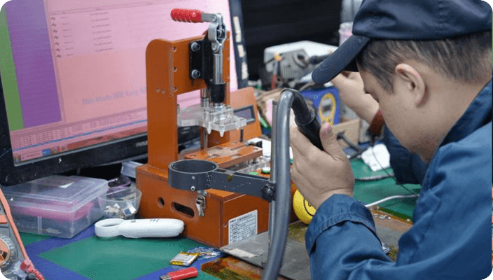 A complete PCBA test plan connects design requirements, test coverage, equipment, quality records, and mass production control.