Phone: +86-137 5102 2384
Phone: +86-137 5102 2384
Oct. 19, 2026
Share:
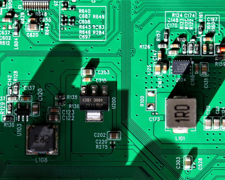
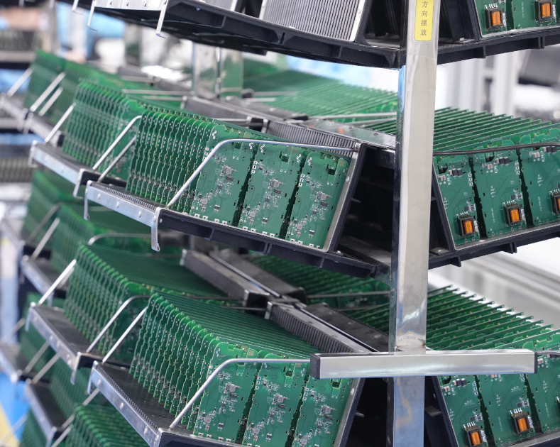
Double-sided SMT assembly requires careful component placement, PCB support planning, and thermal management to ensure that components on both sides of a printed circuit board (PCB) remain correctly positioned through two soldering stages. Heavy components, bottom-side clearance, reflow temperature profiles, and inspection access all influence the final design. Before production, buyers should review these factors with their assembly supplier and evaluate the board through design-for-manufacturing (DFM) checks. Benewave’s one-stop PCB assembly service integrates PCB fabrication, component sourcing, SMT and DIP assembly, programming, and testing to help coordinate manufacturing requirements for complex electronic assemblies.
In single-sided SMT assembly, components are mounted and soldered on one side of the PCB. Double-sided assembly adds a second placement and reflow stage, which means the first side must remain secure while the opposite side is processed.
A typical process includes solder paste printing, component placement, and reflow for Side A, followed by the corresponding operations for Side B. The exact sequence may vary with the board design and component mix.
During the second reflow, Side A components face downward. Molten solder surface tension can hold many components in place, but retention depends on component mass, package geometry, solder-joint design, and process conditions. It should not be assumed that every component will remain secure without additional planning.
For this reason, double-sided SMT design must balance electrical routing with mechanical stability, thermal behavior, and manufacturing access.
Larger BGAs, heavy inductors, transformers, and certain connectors may be better candidates for the first assembly side, especially when their mass or geometry makes bottom-side retention more challenging.
However, component weight alone does not determine placement. The solder-joint configuration, package size, number of joints, surface tension during reflow, and the temperature requirements of the components all matter.
A heavy component may require a specific process strategy rather than simply being assigned to Side A. Through-hole components or parts with special mechanical requirements may also need DIP assembly or another mounting method.
Small resistors, capacitors, and other lightweight surface-mount components are often suitable for the second side when the design and assembly process support them.
For example, 0402 and 0603 passive components are common in compact electronic assemblies. Their suitability for Side B still depends on solder-joint geometry, component spacing, board orientation, and the supplier's validated process.
For high-density designs, Benewave's SMT and DIP assembly service can support process planning for mixed component types. Buyers should provide the BOM and assembly drawings so that component placement and mounting methods can be reviewed before production.
Double-sided assembly introduces mechanical constraints that may not exist on a single-sided board. During the second assembly stage, previously soldered components on Side A face the support tooling or conveyor system. If the board is not supported correctly, tall or fragile parts can be damaged.
The PCB layout should leave sufficient space for support pins, fixtures, or other tooling used during placement and reflow. The required clearance depends on board dimensions, component heights, panelization, and the equipment used by the manufacturer.
When a component protrudes from Side A, the supplier may need to adjust support locations or design a custom fixture. This is particularly important for thin boards, flexible circuits, and assemblies with components distributed across most of the available area.
Before releasing the design, ask the assembly supplier to review:
Components that may interfere with support tooling.
Board edges and conveyor rail clearance.
Fixture access beneath tall or fragile parts.
Whether custom support tooling is required.
Whether the board could flex or deform during handling.
Benewave supports PCB fabrication and assembly across rigid, flexible, and rigid-flex board types. Its PCB assembly capabilities include engineering coordination and production planning, allowing tooling and assembly constraints to be reviewed before a production run.
Component placement should also account for inspection after soldering. Tall components can obstruct the camera's view of nearby joints, while dense layouts can make some areas difficult to inspect or rework.
For bottom-terminated packages such as BGAs, optical inspection alone cannot verify the hidden solder connections. X-ray inspection may therefore be required, depending on the package and the agreed quality plan.
Leave suitable access for inspection where possible, and identify any areas where visual inspection will be limited. This makes it easier to define a practical inspection strategy before production begins.
Double-sided PCB assembly typically involves two reflow stages, so the thermal history of the first side affects the second. Components with different sizes, materials, and thermal masses may heat and cool at different rates.
A large component on Side A directly opposite another large component on Side B can create a locally different thermal profile. However, the result depends on the component construction, copper distribution, PCB thickness, oven settings, and component location. The solution is not always to move large components to opposite areas of the board; it is to verify that the complete assembly can be soldered within the components' permitted process windows.
Component temperature limits: Confirm the permitted reflow profile for each temperature-sensitive part.
Copper distribution: Large copper areas and power planes can change heat transfer across the board.
Component proximity: Dense clusters may heat differently from areas with fewer components.
First-pass solder joints: Ensure the first side remains stable during the second reflow cycle.
Thermal profiling: Validate the actual board temperature at representative locations rather than relying only on the oven's setpoint.
The objective is to establish a reflow profile that provides adequate soldering conditions without exceeding component temperature limits. If the board contains sensitive components, a manufacturer may need to use thermocouples and trial runs to validate the process.
| Design consideration | Single-sided SMT | Double-sided SMT |
|---|---|---|
| Component placement | Components concentrated on one side | Components distributed across both sides |
| Reflow process | Usually one reflow stage for the SMT side | Commonly two reflow stages |
| Component retention | Components are generally supported by the PCB during reflow | First-side components must remain secure during second-side processing |
| Support tooling | Usually simpler | May require additional keep-out zones or custom fixtures |
| Thermal planning | Must account for board and component temperature differences | Must account for both reflow stages and previous thermal exposure |
| Inspection access | Generally easier to plan | Can be restricted by components on the opposite side |
| Design complexity | Often lower for assembly | Requires additional DFM and process review |
| Potential benefit | Simpler manufacturing process | More component placement area within a similar PCB footprint |
Double-sided assembly can increase the usable placement area, but it does not automatically double the number of components that can be fitted. Actual density depends on routing, component clearances, thermal requirements, mechanical constraints, and test access.
A design review before production is generally less expensive than correcting placement or soldering problems after a large batch has been assembled.
Send the supplier the latest Gerber or ODB++ files, BOM, centroid or pick-and-place data, assembly drawings, and relevant component datasheets. Clearly identify which components belong on Side A and Side B.
Confirm that the design files, BOM, and placement data use the same revision. Mismatched revisions can result in incorrect component placement or unexpected assembly requirements.
Design for Manufacturability (DFM) and Design for Assembly (DFA) reviews help identify production risks before the board is built. For double-sided SMT, the review should cover component spacing, package orientation, tooling access, reflow requirements, panelization, and inspection limitations.
For projects requiring integrated production support, Benewave offers one-stop PCB assembly covering board fabrication, electronic component sourcing, SMT and DIP assembly, programming, functional testing, and box-build integration.
Different inspection methods detect different defects. Solder Paste Inspection (SPI) checks solder-paste deposition, AOI identifies many visible placement and soldering defects, and X-ray can inspect suitable hidden solder joints. Electrical and functional tests provide additional verification of circuit performance.
Benewave's published manufacturing capabilities include six SMT lines, three DIP lines, and dedicated functional-testing lines, alongside AOI, X-ray, ICT, and functional-testing options. The appropriate combination should be agreed upon based on the board design, application, and customer acceptance criteria.
A prototype or pilot build can reveal component interference, soldering defects, thermal issues, and fixture requirements before production volume increases. Review the results and resolve any identified issues before approving the final manufacturing process.
This is especially useful for compact wearables, IoT devices, industrial controllers, and other products that combine fine-pitch components with high-density layouts.
Not necessarily. Side A is often a suitable location for components that are difficult to retain during the second reflow, but weight alone is not enough to determine placement. Package geometry, solder-joint design, process conditions, and mechanical requirements must also be considered.
They can, but failure is not inevitable. Solder surface tension can retain many components during reflow, while retention depends on component mass, pad geometry, solder volume, and the condition of the joints. The supplier should assess components with higher retention risk.
No. Some boards can be processed with standard support arrangements. Custom fixtures may be needed when components obstruct support points, the PCB is thin or flexible, or the board geometry makes standard handling unsuitable.
It often introduces additional printing, placement, reflow, handling, and inspection steps, but the total cost depends on the board design, production volume, component mix, and manufacturing process. A DFM review can help identify ways to reduce unnecessary complexity.
Provide the PCB fabrication files, BOM, placement data, assembly drawings, quantities, and any special inspection or testing requirements. Identify large or temperature-sensitive components and disclose any restrictions on reflow, cleaning, or mechanical handling.
If you are planning a double-sided PCB project, contact Benewave at zoe@benewavetech.com to review your component placement, thermal constraints, support tooling, and inspection requirements. Benewave can help coordinate PCB fabrication, component sourcing, SMT/DIP assembly, and testing for prototype builds and volume production.
Find Partners, Not Just Suppliers
Expert OEM & PCBA manufacturing tailored to your exact specifications. Contact us today to discuss your project and discover a more collaborative way to manufacture.
Get a Fast Quote & Free DFM Review
Related PCB Assembly Service