
Phone: +86-137 5102 2384
Phone: +86-137 5102 2384
Jul. 17, 2026
Share:
A PCB assembly leaves the factory in a controlled environment: 23°C, 50% relative humidity, no vibration, stable power, and gentle handling. It then enters a world of thermal extremes, humidity, salt spray, mechanical shock, and electromagnetic noise. The transition is brutal. An automotive engine controller must survive under-hood temperatures cycling between -40°C and +150°C. A base station in a tropical climate operates at 85% RH for years. A drone flight controller endures high-frequency vibration and 50G crash shocks.
Environmental testing is the engineering discipline that bridges this gap. It is not a box-checking exercise for regulatory compliance, nor is it a quality ritual performed before shipment. It is a physics-based validation methodology that subjects PCB assemblies to controlled stressors to reveal failure modes that are invisible under factory conditions: solder joint fatigue, conductive anodic filament growth, substrate delamination, via barrel cracking, and electrochemical migration. When properly integrated into the product lifecycle, environmental testing transforms from a final gate into a predictive tool that drives material selection, process optimization, and design margin validation.
To understand environmental testing, one must first understand the failure mechanisms it seeks to precipitate.
PCB assemblies are composite structures with mismatched coefficients of thermal expansion (CTE). FR-4 laminates expand at approximately 14–17 ppm/°C in the X-Y plane, while ceramic BGA packages expand at 6–7 ppm/°C, and copper traces at 17 ppm/°C. When the assembly undergoes temperature cycling, these mismatches generate shear strain at interfaces—particularly at solder joints, via barrels, and component terminations.
In lead-free SAC305 solder, repeated thermal cycling initiates intergranular cracks in the bulk solder near the intermetallic compound (IMC) layer. The crack propagates with each cycle until electrical continuity is lost. This is the dominant failure mode in electronics subjected to thermal transients. The rate of damage is governed by the Coffin-Manson relationship: the number of cycles to failure is inversely proportional to the plastic strain range raised to a power (typically 1.5–3.0 for solder). This means that increasing the temperature delta accelerates failure nonlinearly—a 100°C cycle does more than twice the damage of a 50°C cycle.
When a PCB operates in humid environments with bias voltage between conductors, two electrochemical failure modes become active:
CAF: Copper ions migrate along the glass fiber/epoxy interface within the substrate, forming a conductive filament from anode to cathode. This creates a resistive short that may initially draw microamps but can progress to catastrophic failure. CAF is accelerated by high humidity, high voltage, and elevated temperature. It is particularly dangerous because it occurs inside the laminate, invisible to surface inspection.
ECM: Metal ions (copper, silver, tin) dissolve from surface conductors in the presence of ionic contamination (flux residue, plating salts) and humidity, migrating toward the cathode and forming dendritic bridges. Unlike CAF, ECM occurs on the board surface or across component packages.
Environmental humidity testing validates that the substrate material, solder mask, and cleaning process are adequate to prevent these mechanisms over the product lifetime.
PCB laminates absorb moisture, plasticize at high temperatures, and degrade when exposed to thermal excursions beyond their glass transition temperature (Tg). Above Tg, the modulus of the resin drops precipitously, and CTE increases dramatically. If the assembly operates above Tg—even transiently—via barrels experience extreme stress, and copper traces may buckle or delaminate. Thermal shock testing (rapid temperature transition) is specifically designed to precipitate these interfacial failures.
Vibration induces fatigue in solder joints, connector contacts, and large components. In industrial and automotive applications, random vibration (5–2000 Hz) causes wire bond fatigue in power modules, BGA ball shear stress, and fretting corrosion in connector interfaces. Mechanical shock (half-sine or trapezoidal pulses) tests the assembly's ability to survive drop, crash, or handling events without component detachment or internal cracking.
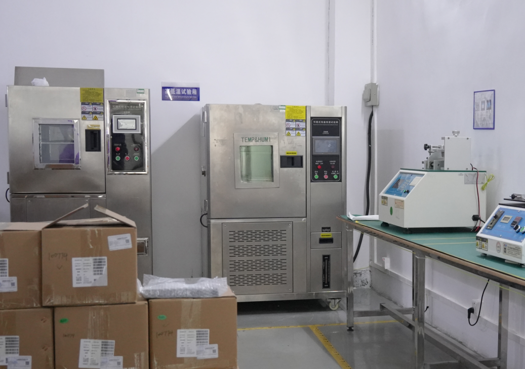
Thermal Cycling (IEC 60068-2-14 / JEDEC JESD22-A104)
Thermal cycling subjects the assembly to repeated transitions between low and high temperature extremes. The critical parameters are:
Temperature extremes: -40°C to +85°C (consumer/industrial), -40°C to +125°C (automotive under-hood), -55°C to +125°C (military/aerospace).
Ramp rate: Typically 5–15°C/minute. Faster ramps generate higher transient thermal gradients and more aggressive stress.
Dwell time: Time at temperature extremes (typically 10–30 minutes) must be sufficient for the assembly to reach thermal equilibrium. Short dwells may not stress large thermal mass components adequately.
Number of cycles: Qualification testing may run 500–1000 cycles. Production screening (ESS) typically runs 10–40 cycles.
Thermal cycling primarily reveals solder joint fatigue, PTH barrel cracks, and component parameter drift. It is the single most important environmental test for PCB assemblies.
Thermal Shock (IEC 60068-2-14, Test Na)
Thermal shock uses a dual-chamber system to transfer the assembly rapidly between hot and cold baths (e.g., 0°C to +100°C liquid, or air-to-air transitions >30°C/min). The extreme thermal gradient generates transient stresses far exceeding those of standard thermal cycling. It is particularly effective at revealing:
Laminate delamination
Via barrel cracking in high-aspect-ratio holes
Die attach failures in power semiconductors
Seal integrity of hermetic packages
High-Temperature Storage (IEC 60068-2-2)
Prolonged exposure to maximum rated temperature (e.g., 1000 hours at +125°C or +150°C) accelerates IMC growth, polymer degradation, and oxidation. It validates long-term material stability but does not induce the mechanical fatigue of thermal cycling.
Steady-State Temperature-Humidity Bias (85°C/85% RH, IEC 60068-2-78 / JEDEC JESD22-A101)
The "85/85" test is the industry baseline for humidity validation. Assemblies are powered under bias voltage at 85°C and 85% relative humidity for 1000 hours. It accelerates both CAF and ECM by providing thermal energy, moisture, and electrical potential simultaneously.
However, 85/85 is slow. For a product with a 10-year life in a 40°C/75% RH environment, 1000 hours of 85/85 may represent only a fraction of the total life stress. It is best used as a qualification benchmark and for comparing material/process changes.
Highly Accelerated Stress Test (HAST, IEC 60068-2-66 / JEDEC JESD22-A110)
HAST operates at 130°C, 85% RH, and 2.3 atm pressure. The elevated temperature and pressure dramatically accelerate moisture ingress and electrochemical reactions. A 96-hour HAST can provide acceleration factors equivalent to 1000+ hours of 85/85. HAST is invaluable for:
Rapid qualification of new laminate materials
Evaluating conformal coating effectiveness
Screening for CAF susceptibility in high-voltage designs
The risk is overstress: if test conditions exceed the material's Tg or glass decomposition temperature, failures may occur that would never happen in the field. HAST must be carefully correlated with field conditions.
Salt Fog / Salt Spray (IEC 60068-2-11 / ASTM B117)
For marine, coastal, and automotive underbody applications, salt fog testing validates corrosion resistance. It exposes assemblies to a 5% NaCl mist at 35°C for 48–96 hours. Post-test evaluation examines solder joint corrosion, connector plating degradation, and conformal coating pinholes.
Vibration (IEC 60068-2-6 Sinusoidal, IEC 60068-2-64 Random)
Sinusoidal vibration: Sweeps through discrete frequencies to identify resonant modes. Useful for identifying natural frequencies of large components (transformers, heatsinks) that may experience amplification.
Random vibration: Simulates real-world vibration with a broadband spectrum (e.g., 5–2000 Hz at 7.7 Grms for automotive). It is more representative of actual service and is the standard for most PCB qualification.
Vibration reveals inadequate component staking, connector retention failures, BGA ball fatigue, and wire bond breakage in power modules.
Mechanical Shock (IEC 60068-2-27)
Half-sine shock pulses (e.g., 50G for 11 ms) simulate drop, crash, and handling events. Post-test inspection checks for component detachment, solder joint cracks, and PCB flexure damage near mounting holes.
Board Flexure (IPC-TM-650, Method 2.4.4)
Specific to PCB assemblies, this test applies a controlled bend (typically 1–2% strain) to the board to validate BGA and large passive solder joint integrity under flexural stress. It is critical for large form-factor boards and handheld devices.
4. Combined and Specialized Environments
Temperature-Vibration Combined (IEC 60068-2-50)
Vibration at temperature extremes reveals failures that neither test alone would catch. Solder is more brittle at low temperature; vibration during cold soak can precipitate cracks that room-temperature vibration misses.
Altitude / Low Pressure (IEC 60068-2-13)
High-altitude and aerospace applications require testing at reduced atmospheric pressure (e.g., 25 kPa, equivalent to 40,000 feet). Low pressure reduces dielectric strength and can trigger partial discharge or arcing in high-voltage assemblies. It also exacerbates outgassing from materials.
Dust and Sand (IEC 60068-2-68)
Validates sealing and conformal coating integrity for outdoor and desert deployments. Fine dust can penetrate enclosures and create conductive paths between biased traces.
Environmental testing is not a monolithic activity. Its purpose, intensity, and risk profile change across the product lifecycle.
During NPI, the goal is to find the breaking point. Tests are often run to failure:
HALT (Highly Accelerated Life Testing): Applies progressively extreme temperatures (often beyond the component ratings) and combined vibration to identify design margins and failure modes. HALT is destructive and not a pass/fail test; it generates knowledge.
Thermal cycling to failure: Running thermal cycles until 63% of the sample population fails generates a characteristic life (Weibull eta) and shape parameter (beta), enabling lifetime prediction under field temperature profiles.
Material qualification: New laminates, solder masks, and conformal coatings are subjected to 85/85, HAST, and thermal shock to validate their suitability for the application.
Once the design is frozen, the goal shifts to catching latent manufacturing defects in production units:
ESS thermal cycling: Typically 10–40 cycles of -40°C to +85°C (or application-specific extremes). This precipitates cold solder joints, insufficient via plating, and component defects without damaging good product.
ESS random vibration: 5–10 minutes per axis at moderate Grms levels to reveal mechanical weaknesses.
Burn-in: Powered operation at elevated temperature (40–60°C above maximum ambient) for 48–168 hours to precipitate infant mortality semiconductor failures.
ESS is a screen, not a qualification. It assumes the design is sound and seeks to remove units with manufacturing defects. It must be carefully profiled: too little stress allows defects to escape; too much stress damages good product (overkill).
For mature products in continuous production, ORT samples units from regular production lots and subjects them to abbreviated qualification testing (e.g., 100 thermal cycles, 168 hours 85/85). ORT detects process drift—changes in solder paste, laminate batches, or component lots that may degrade reliability.
Environmental testing is most powerful when its results feed back into manufacturing process control:
Thermal cycling failure analysis: If failures cluster in BGA corner joints, the feedback loop targets reflow profile optimization (reducing warpage) or underfill implementation.
CAF failures in 85/85: If CAF occurs between specific trace pairs, the feedback loop targets laminate material specification (switching to anti-CAF resin), drill quality, or spacing rules.
Vibration failures: If large capacitors detach, the feedback loop introduces adhesive staking or revised component clamping fixtures.
This closed-loop integration transforms environmental testing from a reactive qualification activity into a proactive process improvement engine.
Running 1000 thermal cycles and recording "3 failures" is useless if the failure mode is not characterized. Was it solder fatigue, pad cratering, or component fracture? Each mode has a different root cause and corrective action. Every environmental test failure must undergo cross-sectioning, dye-and-pry, or SEM/EDS analysis.
Applying -40°C to +85°C because "it is the industrial standard" is negligent if the product operates in a -55°C to +125°C automotive under-hood environment. Test conditions must be derived from the actual field environment, with appropriate acceleration factors and safety margins.
Using HALT-level stresses on production units destroys yield. Using ESS-level stresses for design validation provides false confidence. The test program must clearly separate destructive margin-finding (qualification) from non-destructive defect precipitation (screening).
A single board passing 100 thermal cycles proves nothing. Reliability testing requires statistically significant sample sizes (typically 22–45 units for Weibull analysis) and appropriate confidence intervals. A "qualification" based on three units is not engineering; it is wishful thinking.
Environmental testing is incomplete without full electrical parametric verification after stress. A board may pass visual inspection after thermal cycling but exhibit shifted ADC reference voltages, increased leakage current, or degraded gain bandwidth due to latent material degradation.
Environmental testing is the moment of truth for a PCB assembly. It is where the theoretical robustness of a design meets the physical reality of thermal expansion, moisture ingress, mechanical fatigue, and electrochemical degradation. A board that survives environmental testing with margin is a board that can be trusted in the field. A board that fails in the test chamber has failed in the safest possible way—before it reaches a customer.
The value of environmental testing lies not in the test itself, but in the engineering rigor that surrounds it: accurate field environment characterization, physics-based acceleration models, meticulous failure analysis, and closed-loop feedback to design and process. Manufacturers that treat environmental testing as a regulatory checkbox will continue to experience field failures, warranty claims, and brand damage. Those that treat it as a core engineering discipline—one that validates every material choice, every process parameter, and every design decision—will build products worthy of the most demanding applications.
Thermal cycling (IEC 60068-2-14) transitions the assembly between temperature extremes at a controlled ramp rate (typically 5–15°C/min) with dwell times at each extreme. It is the standard test for solder joint fatigue and is used for both qualification and ESS. Thermal shock uses a dual-chamber system to transfer the assembly rapidly between hot and cold environments (often >30°C/min transition), creating extreme transient thermal gradients. It is more aggressive and is used primarily to reveal laminate delamination, via barrel cracks, and die attach failures that require rapid thermal stress to precipitate. Use thermal cycling for routine reliability validation; use thermal shock when laminate integrity or high-aspect-ratio via robustness is in question.
No, not without careful correlation. HAST (130°C/85% RH/2.3 atm) accelerates moisture-related failures dramatically—often 10–50× faster than 85/85—but the acceleration mechanism may introduce failure modes that do not occur in the field. If the HAST temperature exceeds the laminate's Tg, resin softening may create artificial failures. The standard practice is to use 85/85 for baseline qualification and material comparison (it is the industry-accepted benchmark), and HAST for rapid process change validation or supplier screening. For critical applications, both tests may be required, with HAST results correlated against a historical 85/85 database.
For design qualification, thermal cycling often runs to failure or to a statistically derived life target (e.g., 500–1000 cycles for automotive, 1000+ for aerospace) to generate reliability data and validate design margins. For production ESS, the goal is to precipitate latent manufacturing defects without damaging good product. Typical ESS profiles use 10–40 cycles at the application's temperature extremes. The exact number is determined by screening strength analysis: enough cycles to catch defective solder joints and weak components, but few enough to avoid consuming significant product life. ESS profiles should be validated to ensure they do not remove more than 5–10% of the product's rated thermal fatigue life.
Absolutely not. Environmental testing is a validation and screening tool, not a correction tool. A process that produces 30% cold solder joints cannot be "saved" by ESS; the screen will simply destroy yield by failing most units. Similarly, a design with inadequate creepage spacing cannot be fixed by humidity testing—it will fail, and the test only documents the inevitable. The proper hierarchy is: (1) design for reliability, (2) control the manufacturing process via SPC to produce inherently robust product, and (3) use environmental testing to validate the design and catch the small fraction of units with latent manufacturing defects. Testing does not build quality; it verifies that quality was built.
Conductive Anodic Filament (CAF) is the most commonly missed and most destructive latent failure mode. It occurs inside the PCB substrate, along glass fiber bundles, and produces no visible surface indication until it bridges conductors and causes a short. Standard visual inspection, AOI, and even ICT may miss it entirely. CAF is detected through biased humidity testing (85/85 or HAST with DC voltage applied between adjacent conductors) followed by insulation resistance monitoring. A drop in insulation resistance between test points indicates ionic migration. Post-failure analysis requires cross-sectioning at the failure location to visualize the copper filament within the laminate. Prevention requires anti-CAF laminate materials, adequate conductor spacing, and clean drilling processes that do not fracture glass fibers.
Find Partners, Not Just Suppliers
Expert OEM & PCBA manufacturing tailored to your exact specifications. Contact us today to discuss your project and discover a more collaborative way to manufacture.
Get a Fast Quote & Free DFM Review
Related PCB Assembly Service







