
Phone: +86-137 5102 2384
Phone: +86-137 5102 2384
Jun. 10, 2026
Share:
A Professional Guide to DFM, Process Control, and IPC Standards
Industry Case Study: John, a professional PCB manufacturing engineer, once faced a staggering 15% failure rate in a production batch due to incorrect component placements. This costly error delayed shipments and highlighted the urgent need for robust quality control systems to stop PCB assembly defects before they reach the testing phase.
In printed circuit board assembly (PCBA), early identification of potential defects is the first step toward robust quality control. These defects typically manifest during the soldering, placement, or surface finish stages:
Solder Joint Defects: Cold solder joints, voids, and solder bridging are the most prevalent issues. In unoptimized processes, cold or insufficient solder joints can lead to a testing failure rate of up to 20%.
Tombstoning: This occurs during reflow soldering when a passive component (such as a 0402 or 0603 resistor/capacitor) stands up on one end. It is caused by an imbalance in surface tension when the solder paste on one pad melts faster than the other.
Component Misplacement & Polarity Issues: Especially in high-density, complex designs, incorrect component placement or reversed polarity can cause immediate board malfunction, with failure rates exceeding 30%.
Surface Finish Degradation: Inadequate surface finishes (e.g., OSP, ENIG, or HASL) lead to oxidation and corrosion, which can shorten the operational lifespan of the PCB by up to 50%.
High-yield PCB assembly relies on rigorous pre-production preparation and strict Design for Manufacturability (DFM) guidelines:
Premium Substrates and Consumables: Always source high-quality bare boards from industry-leading suppliers like Benewave, and pair them with high-grade lead-free solder paste (e.g., SAC305).
Precision Thermal Equipment: Multi-zone reflow ovens with precise temperature profiling and ESD-safe, temperature-controlled soldering irons.
Advanced Inspection Instruments: 3D Solder Paste Inspection (SPI) systems, Automated Optical Inspection (AOI) machines, and high-definition inspection microscopes.
Symmetrical Pad Design: Ensure that both pads of chip components are completely identical in size, trace connection width, and thermal relief. This symmetrical heat absorption prevents tombstoning.
Solder Mask Dam Implementation: Maintain a solder mask dam of at least 0.1mm between adjacent pads. This physical barrier prevents molten solder from flowing together, eliminating solder bridging.
Unambiguous Polarity and Fiducial Markings: Clearly define cathode/anode orientations for polarized components (such as diodes and electrolytic capacitors) on the silkscreen layer, and mark Pin 1 clearly. Additionally, place global and local fiducial marks to allow high-precision pick-and-place alignment.
For modern lead-free assembly using SAC305 solder paste (which has a liquidus temperature of approximately 217℃, the reflow profile must be strictly controlled to prevent cold joints and thermal damage:
Preheating Stage: Maintain a ramp-up rate of 1.0℃/s to 3.0℃/s to gently evaporate solvents and prevent component thermal shock or solder splattering.
Soak/Activation Stage: Keep the temperature between 150℃ and 200℃ for 60 to 120 seconds. This allows the flux to fully activate and remove surface oxides.
Peak Temperature: The profile must reach a peak temperature of 235℃ to 245℃ (never drop below 230℃ as it causes incomplete wetting, and never exceed 260℃ to avoid component damage).
Time Above Liquidus (TAL): The duration above 220℃ must be strictly controlled between 40 and 90 seconds (optimally 60 seconds) to form a healthy, reliable Intermetallic Compound (IMC) layer.
| Defect Type | Root Cause Analysis | Professional Prevention Strategy |
| Cold Solder Joint | Insufficient peak reflow temperature or too short Time Above Liquidus (TAL), preventing proper alloy bonding. | Calibrate reflow ovens regularly. Ensure peak temperatures reach 235℃ - 245℃ and TAL stays between 40–90 seconds for SAC305. |
| Solder Bridging | Excessive solder paste deposition, poor stencil aperture design, or lack of solder mask dams. | Use laser-cut, electro-polished stencils with optimized aperture reduction. Ensure a minimum 0.1mm solder mask dam between pads in the design. |
| Tombstoning | Asymmetric pad dimensions or trace routing, causing uneven heat distribution and unbalanced surface tension. | Optimize DFM layout so that trace widths and thermal relief connections are identical on both sides of passive components. Use 3D SPI to check paste volume consistency. |
| Polarity Issues | Confusing silkscreen design, incorrect pick-and-place programming, or lack of pre-production verification. | Standardize silkscreen polarities in your CAD library. Execute a First Article Inspection (FAI) using automated testers before starting mass production. |
To consistently achieve high yields, manufacturers should adopt this 5-step quality loop:
DFM Review: Run comprehensive design rule checks on component clearances, footprint accuracy, and trace thermal paths before sending files to fabrication.
Solder Paste Printing & SPI: Since roughly 70% of all assembly defects stem from poor solder paste printing, 3D SPI must be used to instantly reject and clean boards with height or volume deviations.
First Article Inspection (FAI): Prior to mass-producing a batch, assemble and reflow a single board. Use an FAI system to verify component values, orientations, and polarities against the Bill of Materials (BOM).
Precision-Profiled Reflow: Use multi-zone reflow profiles tailored to the thermal mass of the board, verified by a thermal profiler pass-through.
Automated Optical Inspection (AOI): Post-reflow, use AOI to scan 100% of the batch for bridges, tombstoning, and alignment issues, ensuring a defect escape rate of less than 1%.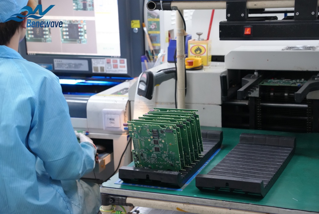
Minimizing defects in PCB assembly is a science that combines high-quality materials with rigorous process control. By sourcing premium bare boards from trusted manufacturers like Benewave, aligning assembly lines with IPC-A-610 standards, and utilizing closed-loop testing (SPI, FAI, and AOI), you can dramatically reduce rework costs and improve product reliability.
In professional electronics manufacturing, defect rates are typically measured in PPM (Parts Per Million). Top-tier EMS providers target a First Pass Yield (FPY) of over 99% (equivalent to a process defect rate of under 1%), with high-reliability aerospace or automotive lines targeting 6-Sigma quality standards (3.4 defects per million opportunities).
FAI is a proactive preventive measure, whereas AOI is a reactive screening tool. FAI verifies that the correct components are loaded onto the correct feeders before the machine runs the entire batch, preventing systematic errors. AOI checks the quality of the physical solder joints and placement alignment across the entire production run.
Traditional tin-lead solder (Sn37Pb) has a eutectic temperature of only 183℃. Modern lead-free alloys (such as SAC305) have a higher melting point of 217℃. Because of this, the peak reflow oven temperature must be elevated to 235℃- 245℃ to ensure the lead-free alloy fully melts, wets, and forms a reliable mechanical and electrical connection.
Find Partners, Not Just Suppliers
Expert OEM & PCBA manufacturing tailored to your exact specifications. Contact us today to discuss your project and discover a more collaborative way to manufacture.
Get a Fast Quote & Free DFM Review
Related PCB Assembly Service







